Why Chip Fab Wastewater Defeats Conventional Treatment Systems
Chip fab wastewater in 2026 demands hybrid systems because influent pH swings between 2.0 and 12.0 within 60 to 120 minutes, while TMAH (10–100 mg/L), fluoride (50–300 mg/L), and silica (>200 mg/L) all exceed the design envelope of standard industrial plants. For a 5 MGD fab, the train resolves to DAF for 95%+ TSS removal, a zero-fouling MBR with 0.1 μm filtration, RO for 90% water recovery, and AOP polishing, with CAPEX typically ranging from $5M–$50M depending on redundancy and automation.
Advanced node semiconductor manufacturing generates wastewater that conventional plants cannot handle because those plants are sized for steady-state organic loads. A semiconductor fab wastewater treatment system has to absorb rapid swings between hydrofluoric acid (HF) etching cycles and alkaline cleaning steps. Automated chemical dosing must deliver sulfuric acid or caustic soda at 0.5–2 L/min to hold a stable influent pH for downstream biology. The organic profile is dominated by Tetramethylammonium Hydroxide (TMAH), a developer that is both toxic to standard nitrifiers and resistant to plain aeration. Many fab streams are "zero-nutrient," with BOD often falling below 50 mg/L, so carbon dosing at 20–50 mg/L acetate is required to prevent biomass washout. Silica (>200 mg/L) and fluoride (50–300 mg/L) force precipitation or ion exchange upstream of RO to control scaling. Most plants we size for 28 nm and below nodes run at the lower end of those contaminant ranges, with pH transients as the dominant upset driver.
Hybrid System Design: DAF + MBR + RO + AOP for Chip Fab Design
A comprehensive hybrid system, integrating Dissolved Air Flotation (DAF), Membrane Bioreactors (MBR), Reverse Osmosis (RO), and Advanced Oxidation Processes (AOP), is essential for achieving zero-discharge compliance in chip fab wastewater treatment. This multi-stage approach systematically addresses the complex contaminant profile characteristic of semiconductor fabrication facilities.
Stage 1: Dissolved Air Flotation (DAF) initiates the treatment process by removing over 95% of Total Suspended Solids (TSS) and approximately 80% of Fats, Oils, and Grease (FOG). Utilizing micro-bubble technology, a high-efficiency DAF system for TSS and FOG removal in semiconductor fabs can achieve surface loading rates of 40–60 m/h, effectively preparing the influent for subsequent biological treatment.
Stage 2: Zero-Fouling MBR employs 0.1 μm PVDF membranes to provide robust biological treatment. This MBR Membrane Bioreactor Wastewater Treatment System effectively reduces Chemical Oxygen Demand (COD) to below 50 mg/L and TMAH concentrations to less than 1 mg/L. Integrated aeration scouring is a critical feature of these advanced DF series flat sheet modules, which significantly mitigates membrane fouling and extends operational cycles.
Stage 3: Reverse Osmosis (RO) is employed for high-purity water recovery, achieving up to 90% water reclamation. An anti-scalant dosing strategy is crucial within the RO system for 90% water recovery in semiconductor fab wastewater reuse to prevent silica fouling, ensuring sustained performance and membrane longevity. Refer to the RO membrane selection guide for semiconductor wastewater reuse for detailed considerations.
Stage 4: Advanced Oxidation (AOP) targets any residual refractory organic compounds. UV/H₂O₂ oxidation, for instance, can achieve up to 99% TMAH degradation with a UV dose of 500–1000 mJ/cm², aligning with EPA 2024 benchmarks for effective tertiary treatment.
The following table illustrates the typical influent and effluent quality at each stage of a DAF-MBR-RO-AOP hybrid system:
| Treatment Stage | Influent (Typical) | Effluent (Typical) | Key Contaminants Removed |
|---|---|---|---|
| Raw Wastewater | pH: 2.0–12.0 TSS: 100–500 mg/L COD: 100–500 mg/L TMAH: 10–100 mg/L Fluoride: 50–300 mg/L Silica: 50–250 mg/L |
- | - |
| DAF | (See Raw Wastewater) | TSS: <10 mg/L FOG: <10 mg/L COD: 80–400 mg/L |
TSS, FOG |
| Zero-Fouling MBR (0.1 μm) | TSS: <10 mg/L COD: 80–400 mg/L TMAH: 5–50 mg/L BOD: <50 mg/L |
COD: <50 mg/L TMAH: <1 mg/L BOD: <10 mg/L |
COD, BOD, TMAH (biological degradation), Colloidal Solids |
| RO (90% Recovery) | TSS: <1 mg/L TDS: 500–2000 mg/L Silica: <50 mg/L |
TDS: <10 mg/L Silica: <5 mg/L Recovered Water: 90% |
TDS, Dissolved Salts, Heavy Metals, Silica |
| AOP (UV/H₂O₂) | COD: <50 mg/L TMAH: <1 mg/L Residual Organics |
COD: <10 mg/L TMAH: <0.1 mg/L Trace Organics: Degraded |
Refractory Organics, Pesticides, Pharmaceuticals (if present) |
An automated pH dosing system for chip fab wastewater treatment is integral to maintaining optimal performance across all stages, particularly before the MBR and RO units.
Zero-Fouling MBR vs. Conventional MBR: Energy, Lifespan & OPEX Comparison
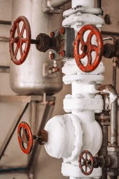
For semiconductor fab wastewater treatment, the selection of a Membrane Bioreactor (MBR) system significantly impacts operational efficiency and long-term costs. Zero-fouling MBR technology offers substantial advantages over conventional MBR designs in terms of energy consumption, membrane lifespan, and overall Operating Expenditure (OPEX).
Zero-fouling MBR systems typically exhibit energy consumption ranging from 0.4–0.6 kWh/m³, a marked improvement compared to conventional MBRs, which can consume 0.8–1.2 kWh/m³. This reduction is largely attributed to optimized aeration strategies and advanced membrane surface treatments that minimize drag resistance. The lifespan of membranes in zero-fouling systems is considerably longer, often reaching 8–10 years, whereas conventional membranes typically last 3–5 years. This extended lifespan translates to a direct reduction in replacement OPEX by approximately 60%.
The efficacy of TMAH removal is also a critical differentiator. Zero-fouling MBRs can achieve 99% TMAH removal, which is crucial for meeting stringent EPA NPDES compliance limits (<1 mg/L). Conventional MBRs, while capable of biological treatment, may struggle to consistently achieve such high removal rates for recalcitrant compounds like TMAH, often requiring post-treatment. The compact design of zero-fouling MBRs also results in a smaller footprint, often 60% less than conventional systems, making them ideal for space-constrained semiconductor fabrication facilities or retrofit projects.
Fouling mechanisms in MBRs, such as biofouling and scaling, are aggressively mitigated in zero-fouling designs through inherent material properties and operational strategies. Automated Chemical-Enhanced Backwashing (CEB) and integrated aeration scouring, as found in DF series flat sheet modules, are key to maintaining low transmembrane pressure and extending membrane performance. This proactive approach reduces the frequency and intensity of manual cleaning, further lowering OPEX and labor requirements.
| Parameter | Zero-Fouling MBR | Conventional MBR | Impact on Chip Fab Wastewater |
|---|---|---|---|
| Energy Consumption (kWh/m³) | 0.4–0.6 | 0.8–1.2 | Lower energy costs, reduced carbon footprint |
| Membrane Lifespan (Years) | 8–10 | 3–5 | Reduced replacement CAPEX/OPEX, less downtime |
| TMAH Removal (%) | 99% | 90% | Higher assurance of meeting strict discharge limits |
| OPEX Reduction (vs. Conventional) | 30–40% | N/A | Significant long-term cost savings |
| Footprint Reduction | ~60% | N/A | Enables installation in space-constrained facilities |
| Fouling Mitigation | Automated CEB, Aeration Scouring, Advanced Surface Treatments | Periodic manual cleaning, standard aeration | Higher operational reliability, reduced maintenance |
CHIPS Act Compliance: EPA NPDES, Local Reuse Targets & Permit Requirements
For semiconductor fabrication facilities funded by the CHIPS Act, stringent wastewater treatment and discharge compliance are paramount. Understanding and mapping these requirements to specific treatment design parameters ensures successful project execution and avoids costly non-compliance penalties.
The U.S. Environmental Protection Agency (EPA) sets National Pollutant Discharge Elimination System (NPDES) limits for semiconductor manufacturing wastewater. Key parameters include a limit for Total Suspended Solids (TSS) of <30 mg/L, fluoride of <4 mg/L, and Tetramethylammonium Hydroxide (TMAH) of <1 mg/L, as outlined in 40 CFR Part 469. These limits dictate the performance targets for the wastewater treatment system.
Beyond federal regulations, CHIPS Act projects must also adhere to ambitious local water reuse targets. For example, states like Arizona aim for 75% water reuse, Texas targets 85%, and California pushes for 90%. Achieving these targets requires advanced treatment technologies, such as RO, to produce high-quality recycled water suitable for various process applications. For more insights on achieving high recovery rates, consult the RO membrane selection guide for semiconductor wastewater reuse.
Permit application processes for CHIPS Act-funded facilities typically demand detailed documentation. This includes comprehensive influent and effluent quality data, robust redundancy plans for critical treatment systems (such as a backup MBR train), and established monitoring protocols for key parameters like pH, TSS, and TMAH. Common permit pitfalls include underestimating the impact of high silica concentrations (>200 mg/L) on RO membrane scaling or failing to design biological systems that can effectively handle rapid pH swings (2.0–12.0) inherent in fab operations. Understanding the engineering specs for etching wastewater treatment in semiconductor fabs is crucial for this preparation.
| Regulatory Requirement | Specific Parameters/Targets | Implication for Design |
|---|---|---|
| EPA NPDES Limits (40 CFR Part 469) | TSS: <30 mg/L Fluoride: <4 mg/L TMAH: <1 mg/L |
Requires high-efficiency TSS removal (DAF), fluoride precipitation/ion exchange, and advanced biological/AOP for TMAH. |
| Local Water Reuse Targets (State-Specific) | Arizona: 75% Texas: 85% California: 90% |
Mandates high-recovery technologies like RO, requiring careful pre-treatment to prevent fouling and robust post-treatment for reuse quality. |
| CHIPS Act Permit Applications | Influent/Effluent Data Redundancy Plans Monitoring Protocols |
Demands detailed system design documentation, fail-safe mechanisms for critical units, and continuous performance tracking. |
| Common Permit Pitfalls | Silica Scaling in RO (>200 mg/L) pH Swings (2.0–12.0) in Biological Systems TMAH Toxicity to Microbes (10–100 mg/L) |
Requires robust pre-treatment for silica, automated pH control, and specialized biological processes (e.g., zero-fouling MBR). |
CAPEX & OPEX Cost Model: $5M–$50M for 5 MGD Chip Fab Wastewater Treatment
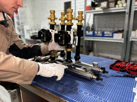
The Capital Expenditure (CAPEX) for a 5 MGD chip fab wastewater treatment system typically ranges from $5 million to $50 million, heavily influenced by system complexity, the degree of redundancy, and the integration of advanced technologies like zero-fouling MBRs and RO. Operational Expenditure (OPEX) generally falls between $0.80 and $1.50 per cubic meter of treated water.
A breakdown of CAPEX for a 5 MGD hybrid system might include: DAF units ($1M–$3M), MBR systems ($2M–$8M, with zero-fouling designs potentially at the higher end), RO units ($1.5M–$5M), AOP systems ($0.5M–$2M), and automation and control systems ($1M–$3M). These figures are indicative and can vary significantly based on specific site requirements and vendor selection. For a comprehensive understanding of related costs, the engineering specs for etching wastewater treatment in semiconductor fabs can provide additional context.
OPEX components include energy costs ($0.30–$0.50/m³), which are lower with energy-efficient technologies like zero-fouling MBRs; membrane replacement and maintenance ($0.20–$0.40/m³), where zero-fouling MBRs offer significant savings; and chemical dosing ($0.10–$0.20/m³) for pH adjustment, disinfection, and anti-scalants. The return on investment (ROI) for these systems is driven by several factors: water reuse, which can reduce municipal supply costs by 50–70%; CHIPS Act tax credits, potentially covering up to 30% of CAPEX; and the avoidance of fines for NPDES violations, which can range from $25,000 to $100,000 per incident.
Cost-saving strategies can be implemented through modular system designs, allowing for phased expansion as fab capacity grows, and by selecting energy-efficient blowers for MBR aeration. The detailed engineering specifications for TMAH wastewater treatment can also inform cost-effective design choices, as explored in the detailed engineering specs for TMAH wastewater treatment.
| Cost Component | Estimated Range (5 MGD System) | Cost Drivers/Savings Opportunities |
|---|---|---|
| CAPEX | $5M–$50M | System complexity, redundancy, technology choice (zero-fouling MBR, RO), automation |
| DAF | $1M–$3M | Flow rate, TSS load, automation level |
| MBR (Zero-Fouling) | $2M–$8M | Membrane area, module type, redundancy, pre-treatment integration |
| RO | $1.5M–$5M | Recovery rate, water quality requirements, pre-treatment effectiveness |
| AOP | $0.5M–$2M | Treatment intensity, contaminant type, reactor design |
| Automation & Controls | $1M–$3M | SCADA integration, sensor density, safety interlocks |
| OPEX | $0.80–$1.50/m³ | Energy prices, chemical consumption, membrane lifespan, labor costs |
| Energy | $0.30–$0.50/m³ | Efficiency of blowers, pumps, UV lamps; zero-fouling MBRs reduce blower energy |
| Membrane Replacement & Maintenance | $0.20–$0.40/m³ | Zero-fouling MBRs significantly reduce frequency and cost |
| Chemicals | $0.10–$0.20/m³ | pH adjustment chemicals, anti-scalants, cleaning agents |
| ROI Drivers | Water Reuse Savings (50–70%) CHIPS Act Tax Credits (up to 30% CAPEX) Avoided Fines ($25K–$100K per incident) |
Maximizing water reuse, leveraging available incentives, ensuring compliance |
Vendor Selection Framework: 5 Critical Questions for Chip Fab Wastewater Treatment Suppliers
Selecting the right vendor for semiconductor fab wastewater treatment is critical to ensuring system reliability, compliance, and cost-effectiveness. Procurement teams should employ a structured framework, asking targeted questions to rigorously evaluate potential suppliers and mitigate selection risks.
1. Case Studies & Experience: "Can you provide detailed case studies of semiconductor fab wastewater treatment systems you have designed and implemented that handle similar contaminant profiles, specifically addressing TMAH (10–100 mg/L), fluoride (50–300 mg/L), and silica (>200 mg/L)?" Look for evidence of successful projects in cleanroom environments with comparable process wastewater challenges.
2. System Redundancy & Reliability: "What is your proposed system's redundancy for critical components such as MBR membranes, RO pumps, and disinfection units? How do you ensure continuous operation during maintenance or unexpected downtime?" A robust redundancy plan is essential for uninterrupted fab operations.
3. Compliance & Performance Guarantees: "How does your system design and proposed operation ensure compliance with EPA NPDES limits (e.g., TMAH <1 mg/L) and achieve specific local water reuse targets (e.g., 85% water recovery)? Do you offer performance guarantees for key effluent parameters?" Clear, measurable guarantees are vital.
4. Membrane Lifespan & OPEX: "What is the expected operational lifespan of your MBR and RO membranes, and what is the projected replacement cost per cubic meter of treated water? Are there programs to optimize membrane performance and longevity?" Understanding long-term membrane costs is key to OPEX management.
5. Integrated Solutions & Support: "Do you offer integrated solutions that encompass pre-treatment, biological treatment, advanced polishing, and automation? What level of ongoing technical support, spare parts availability, and training do you provide for semiconductor fab environments?" A vendor with comprehensive capabilities and strong support minimizes operational headaches.
Red flags during vendor evaluation include a lack of specific semiconductor industry references, vague or unqualified compliance guarantees, and an inability to provide detailed performance data for systems treating similar wastewater compositions. Vendors offering solutions that address the specific challenges of high pH swings and toxic organics like TMAH, such as those utilizing advanced zero-fouling MBR system for TMAH and COD removal in semiconductor wastewater technology, should be prioritized.
Who this is for: CHIPS Act-funded fab EPC teams, plant engineers scoping 5 MGD trains, and procurement managers evaluating DAF-MBR-RO bids. Who should look elsewhere: facilities below 1 MGD or non-semiconductor electronics. Next step: send flow and contaminant data to request a sized CAPEX/OPEX quote.
Frequently Asked Questions
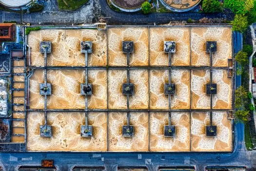
What is the best wastewater treatment system for a new 5 MGD chip fab?
A hybrid DAF-MBR-RO-AOP system is optimal for a 5 MGD chip fab, achieving 95%+ TSS removal in DAF, 99% TMAH degradation across MBR and AOP, and 90% water recovery in RO. CAPEX for such a system ranges from $10M–$30M depending on redundancy and automation levels, with most bids we see landing between $15M and $22M.
How do I comply with CHIPS Act wastewater requirements?
Compliance starts with meeting EPA NPDES limits (TSS <30 mg/L, fluoride <4 mg/L, TMAH <1 mg/L) under 40 CFR Part 469, then layering the state reuse target (e.g., 85% in Texas, 90% in California) on top. Permit submissions must include influent and effluent quality data, redundancy plans for critical trains, and continuous monitoring protocols for pH, TSS, and TMAH.
What are the OPEX costs for a chip fab wastewater treatment system?
OPEX ranges from $0.80–$1.50 per cubic meter of treated water, broken down as energy ($0.30–$0.50/m³), membrane replacement and maintenance ($0.20–$0.40/m³), and chemicals ($0.10–$0.20/m³). Zero-fouling MBR systems reduce OPEX by 30–40% versus conventional designs by extending membrane life from 3–5 years to 8–10 years.
Can I reuse treated chip fab wastewater for process water?
Yes. RO permeate at 90% recovery can be routed to cooling towers, scrubbers, and ultrapure water (UPW) pre-feed with additional polishing such as EDI or mixed-bed ion exchange. Reuse at this level typically reduces municipal water costs by 50–70%, which is the single largest ROI lever for most fabs we model.
What are the biggest risks in chip fab wastewater treatment design?
The three risks that derail most chip fab design projects are underestimating pH swings (2.0–12.0 within 60–120 minutes), silica scaling in RO membranes when influent silica exceeds 200 mg/L, and TMAH toxicity to biomass at 10–100 mg/L. Each is mitigated by automated pH dosing, anti-scalant injection with lime or ion-exchange pre-treatment, and specialized MBR acclimation with carbon supplementation, as detailed in detailed engineering specs for TMAH wastewater treatment.