An electronics wastewater treatment supplier should quote hybrid MBR-RO-DAF trains against measured loads: fluoride 50–500 mg/L, ammonia 20–200 mg/L, Cu 10–100 mg/L — with CAPEX from $200K at 50 m³/day to $10M at 5,000 m³/day.
Why Electronics Wastewater Treatment Demands Custom Engineering
Electronics wastewater carries fluoride at 50–500 mg/L, ammonia at 20–200 mg/L, chelated Cu/Ni/Pb, and UPW brines at 5,000–50,000 mg/L TDS. Lime precipitation alone stalls near 10–20 mg/L fluoride against a sub-4 mg/L target. Custom MBR-RO-DAF trains close the gap at 95–99% contaminant removal.
Semiconductor fabrication plants generate between 2 and 10 cubic meters of wastewater per wafer produced. That flow carries high fluoride (50–500 mg/L) and ammonia (up to 200 mg/L) from etching and cleaning cycles. Plant managers feel the limit most when standard chemical precipitation cannot reach increasingly stringent fluoride discharge numbers set by municipal or federal authorities. Traditional lime softening lands near 10–20 mg/L; the sub-4 mg/L target demands secondary and tertiary polishing that off-the-shelf systems do not provide.
Semiconductor Fab Wastewater Treatment System Selection Criteria
Semiconductor fab wastewater treatment system selection starts from wafer output and rinse chemistry, not from a catalog package. Fluoride branches, ammonia branches, and CMP solids each need their own train before they merge for polishing. Suppliers quoting a single black box against that profile have not read the water balance. Ask for stage-by-stage removal math before the price.
PCB Plating Wastewater Heavy Metal Treatment Sequence
PCB plating wastewater heavy metal treatment runs copper at 10–100 mg/L, nickel at 5–50 mg/L, and lead at 1–10 mg/L. Chelating agents keep those metals dissolved through plain pH adjustment, so the sequence must break complexes first. Specialized chemical dosing for precipitation and pH adjustment doses decomplexer and alkali before solid-liquid separation. Ultrapure water (UPW) production adds brines at 5,000–50,000 mg/L TDS, which demand robust RO or brine concentrators to meet Zero Liquid Discharge (ZLD) goals.
| Contaminant Source | Typical Concentration | Target Discharge Limit (EPA/EU) | Engineering Challenge |
|---|---|---|---|
| Semiconductor Fluoride | 50–500 mg/L | <4.0 mg/L | Solubility limits of CaF₂ |
| Etching Ammonia | 20–200 mg/L | <10.0 mg/L | High toxicity to bio-culture |
| PCB Copper/Nickel | 10–100 mg/L | <0.5 mg/L | Chelated metal complexes |
| UPW Brine (TDS) | 5,000–50,000 mg/L | <500 mg/L (or ZLD) | Membrane scaling and fouling |
Contaminant Removal Benchmarks for Electronics Wastewater
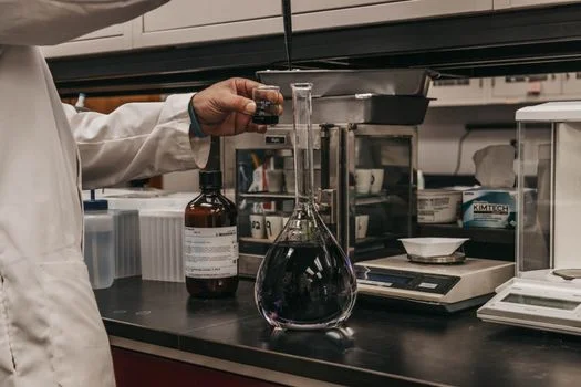
Fluoride Removal Wastewater Semiconductor Path to Sub-4 mg/L
Fluoride removal wastewater semiconductor trains start with calcium hydroxide precipitation, which achieves 80–90% reduction but cannot reach modern compliance benchmarks below 4 mg/L alone. To bridge the gap, engineers deploy RO systems for fluoride and TDS reduction or electrocoagulation as a tertiary step. According to EPA 2024 benchmarks, fluoride removal efficiency must exceed 98% in semiconductor applications for long-term regulatory safety. The sub-4 mg/L target itself tracks the drinking-water frame: EPA's National Primary Drinking Water Regulations list fluoride with an MCL of 4.0 mg/L (US EPA).
Ammonia removal needs a dual-stage approach. Biological nitrification/denitrification removes 95–98% of ammonia at 20–30°C, but high-concentration streams above 100 mg/L require air or steam stripper scrubbers first to protect downstream biology from toxicity (per Saltworks data). Skipping the stripper on an etching branch is how MBR plants lose their biomass in a week.
Heavy metal removal in PCB and electronics lines relies on hydroxide precipitation at a precise pH of 9–10, removing 95–99% of dissolved metals. The resulting micro-flocs are often too light for traditional settling, which is where DAF systems for metals and TSS removal become critical — a high-rate separation step that keeps TSS below 30 mg/L. For facilities aiming at high-quality reuse, ceramic ultrafiltration (such as XtremeUF technology) provides a robust barrier, and the same ceramic membrane water approach removes precipitates at 99% TSS removal with a sub-0.1 μm threshold. That pretreatment protects RO membranes when semiconductor silica exceeds 100 mg/L.
| Technology Type | Primary Contaminant | Removal Efficiency | Key Specification |
|---|---|---|---|
| Chemical Precipitation | Fluoride / Metals | 80–90% | pH 9.2 (Optimum) |
| MBR (Membrane Bioreactor) | COD / Ammonia | 95–98% | 0.1 μm Pore Size |
| DAF (Dissolved Air Flotation) | TSS / Precipitated Metals | 90–99% | 5–10 m³/m²/h Loading |
| Reverse Osmosis (RO) | TDS / Fluoride | 95–99% | 85–95% Recovery Rate |
For organic-heavy streams, MBR systems for electronics wastewater combine biological degradation with membrane filtration. The MBR Membrane Bioreactor Wastewater Treatment System holds biomass at MLSS 8,000–12,000 mg/L, which is vital for degrading the complex solvents and surfactants used in photolithography and cleaning (HydropureWater field data, 2025). Selection detail on effluent quality is covered in the MBR Effluent Quality: Specs, Removal Rates and Selection Guide.
Hybrid System Designs: MBR vs. DAF-RO vs. MBR-RO for Electronics Wastewater
Hybrid system selection depends entirely on the ratio of organic contaminants to inorganic solids. An MBR + RO configuration is the default choice for facilities with high organic loads (COD above 1,000 mg/L) and a need for UPW brine recovery. The MBR removes 95% of COD and TSS while the RO polishes effluent for process reuse, at a CAPEX of $500K to $5M for 100–2,000 m³/day capacities. A DAF + RO system suits PCB manufacturing better, where metal-laden TSS dominates: the DAF unit removes 90% of solids and metals so the RO can focus on fluoride and ammonia with lower fouling risk.
Hybrid MBR-RO-DAF System for Electronics Wastewater: Three Stages
A hybrid MBR-RO-DAF system for electronics wastewater offers the most flexibility for large FABs with variable influent profiles. The MBR handles organic removal, the DAF handles secondary metal and solid separation, and the RO delivers final polishing and ZLD. Integrating a brine concentrator such as the FusionRO pushes RO recovery from 85% to 95% on high-salinity streams, cutting the final evaporation costs of ZLD by 20–30%. Even as production chemistry changes, the three-stage plant stays compliant.
| System Design | Best For... | CAPEX Range | OPEX Impact |
|---|---|---|---|
| MBR + RO | High COD & UPW Reuse | $500K – $5M | High (Membrane Cleaning) |
| DAF + RO | PCB Metals & TSS | $300K – $3M | Moderate (Chemical Costs) |
| MBR + DAF + RO | Semiconductor FAB (ZLD) | $1M – $10M | High (Energy & Recovery) |
CAPEX and OPEX Breakdown for Electronics Wastewater Treatment Plants
Capital expenditure for MBR systems in the electronics sector typically ranges from $4,000 to $6,000 per m³/day of capacity. A mid-sized facility processing 1,000 m³/day faces a $4M investment covering membranes, aeration systems, and high-level automation. DAF systems are more affordable per unit, at $2,000 to $3,500 per m³/day — a small PCB plant with 50 m³/day flow lands near $100K including skimmers and dosing pumps. RO systems fall in the middle at $3,000 to $5,000 per m³/day, driven largely by pretreatment complexity needed to prevent membrane scaling.
Operational expenditure runs on three primary factors: membrane replacement, energy, and chemical dosing. RO membranes require replacement every 3–5 years, while PVDF MBR membranes last 5–7 years with proper maintenance. Energy for these high-pressure and aerated systems runs 0.5–1.5 kWh/m³, and antiscalants plus pH adjusters add $0.10–$0.30 per m³. ZLD systems add 30–50% to initial CAPEX but often pay back within 3–5 years for semiconductor FABs by eliminating discharge fees and cutting raw water procurement by up to 90%.
| Plant Capacity | System Type | Estimated CAPEX | Estimated OPEX ($/m³) |
|---|---|---|---|
| 50 m³/day | DAF + RO (PCB) | $200,000 – $350,000 | $0.45 – $0.75 |
| 500 m³/day | MBR + RO | $2.0M – $3.0M | $0.60 – $0.90 |
| 5,000 m³/day | MBR + DAF + RO (ZLD) | $8.0M – $12.0M | $0.80 – $1.50 |
How to Select an Electronics Wastewater Treatment Supplier: A 5-Step Framework
Choosing an electronics wastewater treatment supplier comes down to five verifiable steps. Semiconductor fabrication plants, PCB manufacturers, and other electronics producers should hold every bidder to the same sequence.
Step 1: Profile your wastewater accurately. Measure fluoride, ammonia, metals, and TDS over a 24-hour composite cycle to capture peak loading rather than averages. Use the benchmarks in this guide to judge whether a supplier's proposed technology is theoretically capable.
Step 2: Define compliance targets in writing. Whether you follow EPA 40 CFR Part 469 categorical limits, Part 433 metal finishing numbers, EU directives, or a local POTW ordinance, pin the governing rule per sewer branch before quoting. Local limits below 0.5 mg/L metals often decide the train, not the federal table.
Step 3: Match technology to contaminant ratios. High COD points to MBR + RO; metals and TSS point to DAF + RO; variable FAB profiles justify the three-stage hybrid. Ask each electronics wastewater treatment supplier to show stage-by-stage removal math against your profile.
Step 4: Verify with pilots and references. A 30-day pilot on real effluent confirms fouling rates and chemical demand before full-scale commitment. Reference plants at comparable scale — chip fab benchmarks appear in the Chip Fab Wastewater Treatment: 2026 Engineering Specs, Zero-Fouling De guide — beat brochure claims every time.
Step 5: Model lifecycle cost, not sticker CAPEX. Compare quotes on $/m³ over ten years: membrane replacement cycles, energy at 0.5–1.5 kWh/m³, chemicals, and ZLD options. Send your composite data, permit limits, and reuse targets through the request-a-quote worksheet for a sized configuration with stage-by-stage budgets.
Frequently Asked Questions
What drives electronics wastewater treatment ZLD system CAPEX?
ZLD CAPEX is driven by the brine branch: concentrators and crystallizers add 30–50% to the base plant cost. Pushing RO recovery from 85% to 95% with tools like FusionRO cuts downstream evaporation costs by 20–30%. Payback runs 3–5 years for semiconductor FABs through eliminated discharge fees and raw water purchases reduced by up to 90%.
How much does a 50 m³/day PCB plant treatment system cost?
A 50 m³/day PCB plant typically invests $200,000–$350,000 in a DAF + RO train, with OPEX at $0.45–$0.75 per m³. The DAF hardware alone lands near $100K including skimmers and dosing pumps. Metal removal to below 0.5 mg/L usually requires decomplexing chemistry ahead of precipitation, so budget chemicals accordingly.
How do you remove fluoride from semiconductor wastewater to below 4 mg/L?
Calcium hydroxide precipitation achieves 80–90% fluoride removal but stalls at 10–20 mg/L. Reaching below 4 mg/L requires a tertiary step — RO or electrocoagulation — after the precipitation stage. Per EPA 2024 benchmarks, overall fluoride removal efficiency should exceed 98% for semiconductor applications.
Which membranes need replacement, and how often?
RO membranes typically need replacement every 3–5 years, while PVDF MBR membranes last 5–7 years with proper maintenance and disciplined CIP. Lifespan tracks pretreatment quality most: DAF or ceramic ultrafiltration ahead of the membranes keeps silica and metals from shortening it. Budget replacement as scheduled CAPEX, not an emergency.
When should a plant choose MBR-RO versus DAF-RO?
Choose MBR + RO when organic load dominates — COD above 1,000 mg/L plus UPW reuse goals — since biology must come before membranes. Choose DAF + RO when metal-laden TSS dominates, as in PCB plating. Variable FAB profiles with both fractions justify the three-stage MBR-DAF-RO hybrid.