Semiconductor wastewater treatment systems must handle high concentrations of dissolved metals (e.g., copper up to 50 mg/L), oxidants like hydrogen peroxide (1,000–5,000 mg/L), and acids (pH 1–3) while meeting EPA 40 CFR Part 469 discharge limits (e.g., copper <1.3 mg/L). Advanced systems like MBR or electrochemical recovery achieve 95%+ water reuse and metal recovery, reducing CapEx by 20–30% compared to traditional precipitation methods. This guide provides 2026 engineering specs, cost models, and compliance strategies for zero-risk implementation.
Why Semiconductor Wastewater Treatment is a $500M/Year Challenge for Fabs
Global semiconductor manufacturing consumes approximately 150–200 million m³ of water annually, with 70% of that volume converted into complex wastewater streams that require multi-stage treatment before discharge or reuse. As the industry transitions to 2nm and 3nm process nodes, the chemical complexity and volume of effluent have increased, transforming wastewater management from a utility function into a $500M/year operational challenge for global fabs. The stakes are increasingly high; regulatory bodies have intensified oversight, with EPA fines for non-compliance reaching up to $50,000 per day for exceedances in copper, fluoride, or arsenic, as mandated under EPA 40 CFR Part 469.
Water scarcity has emerged as a primary threat to production continuity. In Taiwan, the world’s leading semiconductor hub, fabs have recently faced 20% water rationing during extreme droughts, forcing a shift toward aggressive reclamation. Leading manufacturers have set the pace for 2026 sustainability goals; for instance, TSMC’s 2024 Sustainability Report outlines a target of 90% water reuse across all global operations. For a standard 300 mm fab, failing to meet these benchmarks or discharge limits results in more than just financial penalties—it risks the "social license" to operate in water-stressed regions like Arizona or Central Europe.
The financial impact of system failure is best illustrated by a 2023 case study of a 300 mm fab in Arizona. The facility was fined $2.1 million after its traditional precipitation system failed to consistently remove copper from Chemical Mechanical Planarization (CMP) slurry, leading to a discharge exceedance that reached local groundwater. This incident highlights the inadequacy of legacy treatment methods in handling the high-load, variable-chemistry environments of modern wafer manufacturing. To mitigate these risks, procurement teams are now prioritizing systems that offer integrated recovery and real-time monitoring over simple end-of-pipe treatment.
Semiconductor Wastewater Streams: Contaminant Profiles by Process Step
Chemical Mechanical Planarization (CMP) generates the most challenging wastewater stream in the fab, characterized by high concentrations of abrasive silica or alumina particles and dissolved copper ranging from 10 to 50 mg/L. These streams typically maintain a pH of 9–11 (per SEMI S23-0718 standards) and require specialized coagulation and membrane separation to prevent downstream fouling. Effectively managing this stream is critical, as copper is a primary target for EPA enforcement and a valuable candidate for electrochemical recovery.
Etching and wafer cleaning processes contribute high-strength acid and solvent waste. Etching effluent is heavily laden with fluoride (50–200 mg/L) and Tetramethylammonium hydroxide (TMAH), a highly toxic developer with concentrations often reaching 100–300 mg/L. Wafer cleaning stages introduce massive loads of hydrogen peroxide (1,000–5,000 mg/L) and sulfuric acid, resulting in a pH as low as 1–2. Without robust automated chemical dosing for pH adjustment and coagulation, these streams can rapidly degrade treatment infrastructure and biological reactors. Integrating MBR for wafer cleaning wastewater allows for the effective removal of organic solvents and TMAH through targeted aerobic digestion.
| Process Step | Key Contaminants | Concentration Range | pH Range | Avg. Flow Rate (m³/h) |
|---|---|---|---|---|
| CMP (Slurry) | Copper, Silica, Alumina | Cu: 10–50 mg/L; TSS: 100–500 mg/L | 9.0–11.0 | 20–100 |
| Etching | Fluoride, TMAH, Nitric Acid | F: 50–200 mg/L; TMAH: 100–300 mg/L | 2.0–4.0 | 30–150 |
| Wafer Cleaning | H2O2, H2SO4, IPA, Acetone | H2O2: 1k–5k mg/L; COD: 500–2k mg/L | 1.0–2.0 | 50–200 |
| Backgrinding/Rinse | Silicon Fines, Low TSS | TSS: <50 mg/L; Trace metals | 6.5–7.5 | 100–500 |
2026 Engineering Specs for Semiconductor Wastewater Treatment Systems
Modern semiconductor wastewater treatment systems are designed to handle influent COD levels of 500–3,000 mg/L and TSS concentrations up to 1,000 mg/L while meeting 2026 effluent quality targets. The primary goal of these engineering specifications is to ensure that treated water meets the EPA 40 CFR Part 469 standard (copper <1.3 mg/L, fluoride <10 mg/L) and the EU Industrial Emissions Directive 2010/75/EU (COD <125 mg/L). systems must be optimized for water reuse, as new fabs in regions like Taiwan now face mandates for 80% or higher reclamation rates.
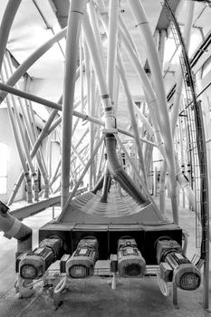
The treatment architecture typically follows a four-stage process. Pretreatment involves high-precision neutralization and equalization to stabilize the wildly fluctuating pH of cleaning and etching streams. The primary stage utilizes Dissolved Air Flotation (DAF) or high-rate sedimentation to remove the bulk of the TSS. The secondary stage is where the most significant technological shifts are occurring; MBR systems for semiconductor wastewater reuse are replacing traditional activated sludge due to their ability to operate at higher biomass concentrations and provide a superior silt density index (SDI) for downstream RO. For ultra-pure water recovery, RO systems for ultra-pure water recovery in fabs are deployed as a tertiary or quaternary step, achieving up to 95% recovery rates.
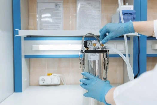
Engineering parameters for 2026 focus on membrane performance and energy efficiency. MBR membranes are specified for a design flux of 15–25 L/m²/h with automated backwash cycles every 10–15 minutes to combat the fouling tendencies of silica-rich CMP waste. RO units are engineered with low-fouling spacers and high-rejection polyamide membranes to handle the residual conductivity of treated fab effluent. For metal-heavy streams, electrochemical recovery cells operate at 99% efficiency, reducing copper to sub-ppm levels before the water even enters the biological stage.
| Technology Type | COD Removal (%) | TSS Removal (%) | Metal Removal (%) | Water Recovery (%) |
|---|---|---|---|---|
| MBR (Membrane Bioreactor) | 95–98% | 99.9% | 40–60% | N/A (Pre-RO) |
| RO (Reverse Osmosis) | 90–95% | >99.9% | 98–99.5% | 75–95% |
| Electrochemical Recovery | <10% | <5% | 99% (Cu/Au) | 98% |
| Fenton’s / AOP | 80–90% | N/A | N/A | 95% |
Treatment Technology Comparison: MBR vs. RO vs. Electrochemical vs. AOP
Membrane Bioreactor (MBR) technology has become the industry standard for treating high-TSS and organic-rich streams from wafer manufacturing. By combining biological degradation with membrane filtration, MBRs consistently produce effluent with COD <50 mg/L and TSS <1 mg/L. This makes them the ideal pretreatment for RO for etching wastewater with fluoride and TMAH, as the MBR permeate significantly extends the lifespan of expensive RO membranes. However, engineers must account for membrane fouling, which requires chemical cleaning (CIP) every 3 to 6 months depending on the silica load.
Reverse Osmosis (RO) remains the backbone of water reuse initiatives, capable of reclaiming up to 95% of treated wastewater for use in cooling towers or as influent for Ultra-Pure Water (UPW) systems. While highly effective, RO carries a higher energy footprint ($0.50–$1.20/m³) and generates a concentrated brine stream that may require further treatment via multi-effect evaporation for ZLD in semiconductor fabs. Electrochemical systems offer a specialized alternative for metal recovery, particularly for copper and gold. Unlike precipitation, which creates hazardous sludge, electrochemical cells recover pure metal plates, turning a waste stream into a revenue source, though they are typically limited to lower flow rates (<50 m³/h).
| Use Case | CapEx ($/m³/h) | OPEX ($/m³) | Pros | Cons | Compliance Fit |
|---|---|---|---|---|---|
| High COD/TSS Removal | $15k–$30k | $0.20–$0.45 | Small footprint, high quality | Membrane fouling risk | Excellent (EU/Taiwan) |
| Water Reuse/Reclamation | $25k–$50k | $0.50–$1.20 | 95% recovery, low TDS | Brine disposal issues | Excellent (ZLD goals) |
| Copper/Metal Recovery | $40k–$80k | $0.15–$0.30 | Zero sludge, pure metal | Limited to <50 m³/h | Best for Cu limits |
| Organic (TMAH) Removal | $20k–$40k | $2.00–$5.00 | Breaks down complex organics | High chemical costs | Required for TMAH |
2026 CapEx and OPEX Benchmarks for Semiconductor Wastewater Systems
Capital expenditure (CapEx) for 300 mm fab wastewater systems typically ranges from $1.5 million to $6 million depending on the required flow rate and treatment complexity. For a mid-sized facility processing 100–500 m³/h, an MBR-based system generally requires an investment of $1.5M–$4M, while a full-scale RO reclamation plant can reach $6M. These costs are heavily influenced by the level of automation and the integration of specialized modules like electrochemical recovery or advanced oxidation for TMAH removal.
Operational expenditure (OPEX) is dominated by energy and chemical consumption, with typical rates ranging from $0.20 to $1.20 per m³ of treated water. Energy costs for MBR and RO systems account for 40–60% of OPEX, while chemical costs for pH adjustment and coagulation contribute 15–25%. However, the Return on Investment (ROI) for these advanced systems is increasingly favorable. In water-stressed regions, the savings from water reuse ($2–$5/m³ compared to municipal freshwater) and the revenue from recovered copper ($10–$50/kg) can lead to a payback period of 3–5 years, particularly when factoring in the avoidance of hazardous sludge disposal costs ($50–$150/ton).
| Fab Size (m³/h) | Typical CapEx ($M) | Avg. OPEX ($/m³) | Treatment Focus | Payback Period (Yrs) |
|---|---|---|---|---|
| 50–100 (Legacy/R&D) | $0.8M–$1.5M | $0.80–$1.50 | Compliance only | 5–7 |
| 100–300 (Standard Fab) | $2.0M–$4.5M | $0.50–$0.90 | Reuse + Compliance | 4–6 |
| 300–800 (Mega Fab) | $5.0M–$12.0M | $0.35–$0.70 | Full ZLD / Reclamation | 3–5 |
Zero-Risk Compliance Blueprint: Aligning with EPA, EU, and Taiwan Standards
The EPA 40 CFR Part 469 standard establishes strict categorical pretreatment limits for the semiconductor subcategory, specifically targeting copper at less than 1.3 mg/L and fluoride at less than 10 mg/L. To ensure zero-risk compliance, fab EHS managers must implement a daily sampling protocol for metals and a weekly protocol for COD and TSS. In the European Union, the Industrial Emissions Directive 2010/75/EU (IED) sets even more stringent "Best Available Techniques" (BAT) benchmarks, requiring COD levels to remain below 125 mg/L and TSS below 35 mg/L for direct discharge into water bodies.
Taiwan’s EPA standards have become the global benchmark for water-stressed manufacturing hubs, recently amending regulations to mandate 80% water reuse for all new semiconductor fabs. Compliance is no longer just about meeting discharge limits; it is about demonstrating resource efficiency. A zero-risk blueprint requires a five-step approach: 1) Comprehensive stream characterization, 2) Technology matching based on the contaminant profile, 3) Pilot testing (typically 3–6 months), 4) Permitting via EPA Form 2C or local equivalents, and 5) The installation of continuous online monitoring for TOC, pH, and conductivity to prevent accidental discharge events.
| Requirement | Regulatory Standard | Action Item | Responsible Party |
|---|---|---|---|
| Copper <1.3 mg/L | EPA 40 CFR Part 469 | Daily composite sampling | EHS Manager |
| Fluoride <10 mg/L | EPA / Taiwan EPA | Calcium precipitation + RO | Operations Team |
| COD <125 mg/L | EU 2010/75/EU | Biological treatment (MBR) | Plant Engineer |
| 80% Water Reuse | Taiwan 2024 Amendment | Tertiary RO + UV treatment | Procurement / EHS |
How to Select the Right Semiconductor Wastewater Treatment System: A Decision Framework
Selecting a treatment system requires a multi-variable analysis that balances initial CapEx against long-term water reuse savings, which currently average $2–$5/m³ in water-stressed regions. The first step in any decision framework is to define the primary goal: is the facility aiming for basic regulatory compliance, maximum water reuse, or the recovery of valuable metals? For most modern fabs, the goal is a hybrid of all three, necessitating a modular approach where different streams are routed to specialized treatment units.
The second step involves characterizing the wastewater in terms of flow rate and chemical variability. If the stream is high-flow (>100 m³/h) and contains high organic loads from cleaning, MBR followed by RO is the most reliable path for reuse. If the stream is low-flow but high in copper, an electrochemical recovery system should be placed upstream of the general treatment plant. Procurement teams should use the 2026 cost benchmarks to evaluate vendors, ensuring that the quoted OPEX includes membrane replacement and chemical consumption. Finally, a 3–6 month pilot test is essential to validate that the selected technology can handle the specific "chemical cocktail" unique to the fab's process recipes.
Decision Tree Summary:
- If goal = Water Reuse and flow >100 m³/h: Select MBR + RO.
- If goal = Metal Recovery and flow <50 m³/h: Select Electrochemical Recovery.
- If goal = TMAH/Organic Removal: Select AOP + MBR.
- If goal = Zero Liquid Discharge (ZLD): Select RO + Multi-Effect Evaporation.
Frequently Asked Questions
What is the typical payback period for a semiconductor wastewater system?
The payback period generally ranges from 3 to 7 years. Systems focused on water reuse and metal recovery pay back faster (3–5 years) due to significant savings on municipal water costs ($2–$5/m³) and the sale of recovered copper ($10–$50/kg). MBR-based systems often show a faster ROI than traditional chemical precipitation due to lower sludge disposal costs and higher effluent quality which protects downstream RO membranes.
Can MBR systems effectively remove TMAH from etching waste?
Yes, MBR systems are highly effective at removing Tetramethylammonium hydroxide (TMAH). Specialized aerobic bacteria in the bioreactor can achieve 99% removal of TMAH when the system is operated at a high Mean Cell Residence Time (MCRT). However, because TMAH is toxic to many microbes, the system must be carefully acclimated during the commissioning phase, often requiring a 4130-etching wastewater treatment by MBR configuration for optimal performance.
Is Zero Liquid Discharge (ZLD) feasible for large-scale semiconductor fabs?
ZLD is technically feasible but carries a high energy and CapEx premium. Most large fabs opt for "Minimum Liquid Discharge" (MLD), achieving 90–95% water recovery. Reaching the final 5% requires evaporators and crystallizers, which can triple the energy cost per m³. ZLD is typically only implemented in regions with absolute discharge prohibitions or extreme water scarcity where the cost of production stoppage outweighs the high OPEX of evaporation.