Why Electronics Wastewater Standards Are Tightening in 2025: A Factory Manager’s Compliance Crisis
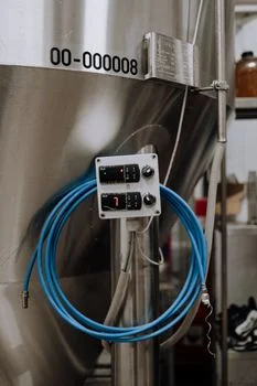
China's GB 39731-2020 sets strict discharge limits for the electronics industry, including fluoride (<15 mg/L), copper (<0.5 mg/L), and total nitrogen (<15 mg/L) for new projects starting January 1, 2021. The EPA's 40 CFR Part 469 and EU Industrial Emissions Directive impose similar but regionally varying limits, requiring advanced treatment systems like MBR (99.9% TSS removal) or ZLD (95%+ water recovery) to achieve compliance. Semiconductor fabs using 10+ million gallons/day of ultrapure water must now close the loop with cost-optimized engineering solutions.
In late 2023, a major semiconductor fabrication facility in Suzhou faced a critical compliance audit that serves as a warning for the industry. Despite having a legacy treatment plant, the facility recorded fluoride levels of 22 mg/L, significantly exceeding the GB 39731-2020 limit of 15 mg/L. The resulting enforcement action led to a mandatory three-month production halt and $2.1 million in cumulative fines and lost revenue. This scenario is becoming increasingly common as China’s 14th Five-Year Plan (2021–2025) targets a 20% reduction in industrial water pollutant discharge, specifically prioritizing the electronics sector due to its high volume of heavy metal and fluoride-rich effluent.
The financial stakes of non-compliance have escalated globally. In China, violations of GB 39731 carry fines up to 1 million RMB ($140,000) per instance, alongside mandatory facility upgrades that often require rapid CAPEX deployment. In the United States, EPA violations under 40 CFR Part 469 can exceed $50,000 per day per violation. Beyond direct fines, manufacturers face reputational damage that can jeopardize Tier-1 supplier statuses with global tech giants who demand strict EHS (Environment, Health, and Safety) adherence.
To navigate this situation, engineering teams must transition from reactive "end-of-pipe" treatment to a proactive 3-step framework. This involves (1) precise mapping of regional pollutant limits, (2) selecting high-efficiency treatment technologies like MBR systems for COD and TN removal in electronics wastewater, and (3) optimizing for both operational cost and water reuse to offset the high CAPEX of advanced compliance systems.
GB 39731 vs. EPA vs. EU: Electronics Wastewater Discharge Limits Compared (2025 Update)
The regulatory landscape for electronics manufacturing is complex, with varying standards across regions.China’s GB 39731-2020 currently stands as one of the most comprehensive and stringent standards globally. While the US EPA’s 40 CFR Part 469 focuses heavily on toxic organics and specific metals, the Chinese standard introduces limits for emerging pollutants like Tetramethylammonium hydroxide (TMAH), which is widely used in semiconductor photoresist developing but often overlooked in older Western regulations. According to global semiconductor wastewater discharge limits for 2025, engineering teams must design systems to the strictest applicable limit if they operate in multiple jurisdictions.
| Pollutant Parameter | China GB 39731-2020 (New Projects) | US EPA 40 CFR Part 469 (Subpart A/B) | EU Industrial Emissions Directive (Typical) |
|---|---|---|---|
| Fluoride (F-) | 15 mg/L | 25 mg/L (Monthly Avg) | 20 mg/L |
| Total Copper (Cu) | 0.5 mg/L | 0.5 mg/L | 0.5 mg/L |
| Total Nitrogen (TN) | 15 mg/L | Not Federally Regulated* | 15 - 25 mg/L |
| COD (Chemical Oxygen Demand) | 60 - 80 mg/L | Site-Specific (NPDES) | 125 mg/L |
| TSS (Total Suspended Solids) | 30 - 50 mg/L | Site-Specific (NPDES) | 35 mg/L |
| TMAH | 5 mg/L | Not Regulated | Varies by Member State |
*Note: EPA limits for TN are often managed at the state level through NPDES permits rather than federal guidelines.
Enforcement mechanisms also differ significantly by region. China’s GB 39731 applies to all new projects approved after January 1, 2021, and existing facilities were required to meet these limits by mid-2023. In the US, the EPA’s guidelines are incorporated into National Pollutant Discharge Elimination System (NPDES) permits for direct dischargers, meaning limits can be even stricter depending on the sensitivity of the local receiving water body. In the EU, the Industrial Emissions Directive (2010/75/EU) uses "Best Available Techniques" (BAT) reference documents to set permit conditions, often pushing for higher water recovery rates than US standards.
Facility type also dictates treatment intensity. Semiconductor fabs, which use massive quantities of hydrofluoric acid for wafer etching, face much higher influent fluoride concentrations (often 500–2,000 mg/L) compared to PCB manufacturers. Consequently, semiconductor wastewater requires two-stage chemical precipitation followed by RO polishing to meet the 15 mg/L GB 39731 limit, whereas PCB electroplating wastewater treatment systems for heavy metal removal focus more on complexed copper and nickel recovery.
Treatment Technologies for Electronics Wastewater: Engineering Specs for 99.9% Pollutant Removal
The primary challenge in electronics wastewater is the co-existence of high-concentration inorganic acids and complex organic solvents. A robust system typically begins with DAF systems for TSS and FOG removal in electronics wastewater pretreatment to protect downstream membranes from fouling.
The 3-tier treatment framework for modern compliance includes:
- Pretreatment: Dissolved Air Flotation (DAF) and chemical precipitation. DAF units achieve 95% TSS removal even at high influent concentrations of 500 mg/L. For fluoride, two-stage calcium chloride dosing is required to drop levels from 1,000 mg/L to <20 mg/L before polishing.
- Biological Treatment: Membrane Bioreactors (MBR) are the industry standard for removing COD and Total Nitrogen. Using DF series membrane specs, MBR systems can maintain high biomass concentrations (MLSS 8,000–12,000 mg/L), ensuring effluent COD remains below 50 mg/L and TN below 10 mg/L (Zhongsheng field data, 2025).
- Polishing and Reuse: RO systems for fluoride and heavy metal removal in semiconductor wastewater provide the final barrier, achieving 95% fluoride rejection and 99% heavy metal removal, making the water suitable for reuse in cooling towers or as feed for ultrapure water (UPW) systems.
| Technology | Removal Efficiency | Energy Consumption (kWh/m³) | Chemical Requirement |
|---|---|---|---|
| DAF (ZSQ Series) | 95% TSS / 90% FOG | 0.1 – 0.3 | PAC/PAM Coagulants |
| MBR (Integrated) | 99.9% TSS / 90% COD | 0.6 – 1.2 | pH adjustment / Carbon source |
| Industrial RO | 95% Fluoride / 99% Metals | 1.5 – 3.0 | Antiscalants / Biocides |
| ZLD (MVR Evaporation) | 99.9% Total Salts | 30 – 50 | Anti-foaming agents |
Process limitations must be factored into the engineering design. For example, semiconductor wastewater often contains high levels of dissolved silica from chemical mechanical polishing (CMP) processes. Silica is a notorious foulant for RO membranes; if influent silica exceeds 20 mg/L, pretreatment must include specialized ion exchange or lime softening. Failure to address silica can increase maintenance costs by 40% due to frequent membrane replacement and cleaning cycles.
Zero Liquid Discharge (ZLD) for Semiconductor Fabs: 2025 Engineering Blueprint with 99% Recovery
Zero Liquid Discharge (ZLD) has moved from a niche environmental requirement to a strategic operational advantage for semiconductor fabs operating in water-stressed regions. By implementing a 4-stage ZLD process, a facility can recover up to 99% of its wastewater, significantly reducing the demand for expensive municipal or raw water. According to ZLD engineering specs, the core of a successful system lies in the efficient management of the brine stream.
The 2025 ZLD Engineering Blueprint is a comprehensive framework.The 2025 ZLD Engineering Blueprint follows this sequence:
- Primary Pretreatment: DAF removes suspended solids and oils, followed by chemical precipitation to reduce fluoride to <15 mg/L. This protects the subsequent biological and membrane stages.
- Secondary Biological: MBR systems treat the organic load (COD/TN). The permeate from the MBR is typically low in solids but high in dissolved salts, making it the perfect candidate for RO.
- Brine Concentration: High-recovery RO systems or Electrodialysis Reversal (EDR) concentrate the salts. To prevent silica scaling, antiscalant dosing and pH adjustment are critical at this stage.
- Thermal Evaporation: Mechanical Vapor Recompression (MVR) is used to treat the final brine. MVR technology is 50% more energy-efficient than traditional multi-effect evaporators, consuming 30–50 kWh/m³ compared to 60–100 kWh/m³.
The cost-benefit analysis for ZLD is heavily influenced by water prices and regulatory pressure. For a 1,000 m³/day system, the CAPEX ranges from $5 million to $12 million. While the OPEX is high ($5–$12/m³), the savings are found in the "closed loop." A facility using 10 million gallons per day of UPW can save over $1.2 million annually in water procurement costs alone by reusing 95% of its effluent. Using chlorine dioxide generators for ultrapure water disinfection within the reuse loop ensures that the recovered water remains free of microbial contamination, protecting sensitive fab processes.
Cost-Optimized Compliance: CAPEX, OPEX, and ROI for Electronics Wastewater Treatment Systems
Selecting a wastewater treatment system for an electronics facility requires a granular understanding of the total cost of ownership (TCO). While conventional treatment systems that meet GB 39731-2020 through discharge have lower CAPEX, they offer no protection against rising water costs or future regulatory tightening. ZLD systems, conversely, have high upfront costs but provide long-term "compliance insurance."
| System Capacity | Conventional CAPEX (USD) | ZLD CAPEX (USD) | Typical OPEX (per m³) |
|---|---|---|---|