Why Microelectronics Organic Wastewater Treatment Demands Specialized Solutions
Microelectronics organic wastewater treatment demands 99.9% removal of tetramethylammonium hydroxide (TMAH) and ammonia to meet EPA and EU discharge limits (e.g., <0.1 mg/L TMAH). Advanced systems combine MBR membranes (0.1 μm pore size) with chemical oxidation (e.g., Fenton’s reagent) to achieve COD reductions from 500–2,000 mg/L to <50 mg/L, while zero liquid discharge (ZLD) systems—costing $1.2–$3.5M for a 50 m³/h fab—eliminate regulatory risks by recovering 95%+ of wastewater for reuse. This guide provides 2025 engineering specs, cost breakdowns, and compliance-ready equipment pairings.
The unique chemical profile of semiconductor effluent makes generic industrial treatment systems, such as standard activated sludge, fundamentally inadequate. TMAH and ammonia are classified as qualitative contaminants; although they may appear in relatively low concentrations compared to municipal waste, their high toxicity and resistance to biological degradation pose extreme risks to aquatic ecosystems. For instance, TMAH is a potent neurotoxin that requires specialized degradation pathways that standard municipal bacteria cannot provide. When these pollutants bypass conventional systems, the financial consequences are severe. A 2023 semiconductor fab in Taiwan faced $2.1M in fines after TMAH exceedances were detected in local waterways, a scenario that highlights the high cost of non-compliance and the necessity for dedicated detailed engineering specs for TMAH wastewater treatment.
microelectronics facilities face high organic load variability, with Chemical Oxygen Demand (COD) fluctuating between 500 and 2,000 mg/L depending on the production cycle. Persistent organic pollutants (POPs), including photoresist residues and fluorinated compounds, are often resistant to traditional aerobic digestion. In regions like Taiwan, Singapore, and the Southwestern United States, water scarcity has accelerated the adoption of Zero Liquid Discharge (ZLD). These systems do not merely treat water for discharge but transform it into a closed-loop resource, mitigating the risk of production halts due to water shortages while ensuring 100% compliance with EPA 40 CFR Part 469.
Pollutant Breakdown: TMAH, Ammonia, and Persistent Organics in Microelectronics Wastewater
Tetramethylammonium hydroxide (TMAH), a primary developer in photolithography, possesses an LD50 of 20 mg/kg (rat oral, per EPA IRIS), making it one of the most hazardous organic components in the electronics manufacturing stream. To protect public health and local infrastructure, effluent limits are increasingly capped at <0.1 mg/L. During the treatment process, the biological or chemical breakdown of TMAH often results in a secondary surge of ammonia-nitrogen. Ammonia is acutely toxic to aquatic life at concentrations exceeding 1 mg/L, necessitating a secondary, high-efficiency nitrification stage to ensure the final effluent meets the EU Water Framework Directive and similar global standards.
Beyond TMAH, the wastewater contains a "cocktail" of persistent organic pollutants (POPs). These include glycol ethers used as solvents, photoresist residues, and various fluorinated compounds that are chemically stable and prone to bioaccumulation. Conventional treatment often fails to break the carbon-fluorine bonds or complex aromatic rings found in these molecules. Therefore, a multi-stage approach is required to address the chemical diversity of the influent. The following table quantifies the typical pollutant profile and the required removal efficiencies for modern semiconductor manufacturing.
| Pollutant Type | Primary Source | Typical Influent (mg/L) | Regulatory Limit (mg/L) | Required Removal Rate |
|---|---|---|---|---|
| TMAH | Photoresist Development | 50–500 | <0.1 (EPA/EU) | 99.9% |
| Ammonia (NH3-N) | TMAH Degradation / Cleaning | 100–500 | <1.0 | 99.5% |
| COD (Total) | Solvents, Resists, Strippers | 500–2,000 | <50 | 97.5%+ |
| POPs | Etching & Stripping | 10–50 | Trace / Non-detect | 99.0% |
Step-by-Step Treatment Process for Microelectronics Organic Wastewater
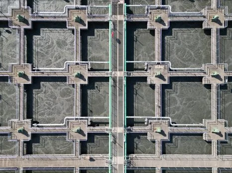
The engineering blueprint for treating microelectronics organic wastewater follows a five-stage progression designed to isolate, degrade, and remove complex molecules while maximizing water recovery. The process begins with Stage 1: Pretreatment. Using rotary mechanical bar screens (GX Series), the system removes >95% of Total Suspended Solids (TSS), such as abrasive silica particles and large photoresist flakes. This step is critical for protecting downstream MBR systems for 99.9% TMAH and ammonia removal in microelectronics wastewater from physical abrasion and fouling.
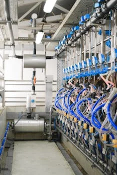
Stage 2: TMAH Removal involves the integration of chemical oxidation and biological treatment. For high-concentration streams, Fenton’s reagent (a mix of hydrogen peroxide and ferrous iron) is utilized to break the TMAH molecule into simpler organic acids and ammonium. This is followed by Stage 3: Ammonia Removal within a submerged Membrane Bioreactor (MBR). Utilizing DF Series membranes with a 0.1 μm pore size, the system maintains a high concentration of nitrifying bacteria. Operating at a flux rate of 20–25 LMH (liters per square meter per hour), these MBR systems achieve 99.9% organic pollutant removal, effectively reducing ammonia from 500 mg/L to <1 mg/L (Zhongsheng field data, 2025).
Stage 4: Persistent Organics treatment utilizes Advanced Oxidation Processes (AOPs), such as UV/H₂O₂ or ozone. These systems generate hydroxyl radicals that attack the remaining recalcitrant COD, ensuring the final organic load is below 50 mg/L. Finally, Stage 5: Zero Liquid Discharge (ZLD) is achieved through high-pressure RO systems for zero liquid discharge (ZLD) in semiconductor fabs followed by evaporation and crystallization. This stage recovers 95%+ of the wastewater for reuse in cooling towers or as ultrapure water (UPW) feed, with a CapEx range of $1.2–$3.5M for a typical 50 m³/h fab configuration.
The equipment pairing for this process flow is as follows: GX Series Mechanical Screens → Precise chemical dosing for TMAH oxidation and pH adjustment → DF Series MBR → UV-AOP → RO Purification → Crystallizer. This sequence ensures that even the most persistent fluorinated compounds and nitrogenous organics are fully mineralized or captured.
Technology Comparison: MBR vs. Conventional Activated Sludge for Microelectronics
Membrane Bioreactors (MBR) have largely superseded Conventional Activated Sludge (CAS) in microelectronics applications due to their ability to maintain high Mixed Liquor Suspended Solids (MLSS) concentrations (8,000–12,000 mg/L) without the risk of sludge bulking. In a semiconductor context, where space is often at a premium and effluent quality is non-negotiable, MBR systems offer a 60% smaller footprint compared to CAS. Because the membrane acts as a physical barrier, the system is not dependent on the settling velocity of bacteria, allowing for 99.9% TMAH removal compared to the 85–90% typically seen in conventional secondary clarifiers.
While CAS systems have a lower initial CapEx ($0.5–$1.2M), their inability to consistently meet <0.1 mg/L TMAH limits often necessitates expensive tertiary polishing filters, which can negate the initial savings. MBR systems, despite a higher CapEx ($1.5–$2.5M), provide much higher flux rates (15–25 LMH) and significantly lower sludge production, reducing long-term disposal costs. For fabs dealing with high-TMAH loads, MBR is the only viable biological solution that guarantees compliance. The following table provides a direct comparison of the two technologies for microelectronics organic wastewater treatment.
| Parameter | MBR System (DF Series) | Conventional Activated Sludge (CAS) |
|---|---|---|
| TMAH Removal Efficiency | 99.9% | 85–90% |
| Ammonia Removal | >99.5% | 90–95% |
| Footprint Requirement | Low (40% of CAS) | High |
| Effluent Turbidity | <0.2 NTU | 2.0–5.0 NTU |
| CapEx (Typical 50 m³/h) | $1.5M – $2.5M | $0.5M – $1.2M |
| Energy Use | 0.6–1.0 kWh/m³ | 0.3–0.5 kWh/m³ |
Zero Liquid Discharge (ZLD) for Microelectronics: Costs, ROI, and Compliance
Zero Liquid Discharge (ZLD) systems for microelectronics represent a strategic investment in regulatory immunity and water security, with CapEx scaling between $1.2M and $3.5M for a 50 m³/h facility. The operational expenditure (OPEX) for these systems typically ranges from $0.8 to $1.5 per cubic meter of treated water. This cost is primarily driven by the energy required for mechanical vapor recompression (MVR) or multi-effect evaporation (MEE) and the chemical dosing required for antiscalants and pH adjustment. Despite these costs, the Return on Investment (ROI) is increasingly favorable as municipal water rates rise and discharge regulations tighten.
The ROI is driven by three primary factors: 95% water recovery, the avoidance of environmental fines ($100K to $2M+ per year), and eligibility for water scarcity credits in regions like Singapore (NEWater) or Taiwan. For example, a 100 m³/h ZLD system in a high-water-cost region can achieve a 2.5-year payback period solely through the reduction in raw water procurement and sewage discharge fees. ZLD eliminates the risk of "stop-work orders" from environmental regulators, which can cost a fab millions in lost production per day. The table below outlines the cost-benefit analysis for ZLD systems based on fab size.
| Fab Size (Flow Rate) | Estimated CapEx | Estimated OPEX ($/m³) | Annual Water Savings (m³) | Typical ROI (Years) |
|---|---|---|---|---|
| Small (10 m³/h) | $400K – $750K | $1.2 – $1.8 | ~83,000 | 4.0 – 5.0 |
| Medium (50 m³/h) | $1.2M – $3.5M | $0.8 – $1.5 | ~415,000 | 3.0 – 4.0 |
| Large (200 m³/h) | $6.0M – $12.0M | $0.6 – $1.1 | ~1,660,000 | 2.0 – 3.0 |
Selecting the Right Equipment for Microelectronics Organic Wastewater Treatment
Choosing the correct equipment requires a decision framework that balances fab capacity, pollutant concentration, and local discharge mandates. For small-scale facilities or back-end packaging plants with flow rates below 20 m³/h and low COD levels, an underground integrated sewage treatment plant (WSZ Series) combined with basic chemical dosing may suffice for compliance. However, for front-end wafer fabrication where TMAH and ammonia loads are substantial, a high-performance MBR system is the industry standard. These systems provide the necessary biological stability to handle the toxic shocks common in semiconductor manufacturing.
When selecting a vendor, engineering teams should utilize the following checklist to ensure the proposed system meets 2025 compliance standards:
- Does the system guarantee 99.9% TMAH removal at influent concentrations of 200 mg/L?
- What is the design flux rate for the MBR membranes (should be 15–25 LMH for microelectronics)?
- Is the AOP stage optimized for the specific persistent organics (e.g., glycol ethers) present in your process?
- What are the energy recovery options for the ZLD evaporation stage?
- Does the vendor provide real-time monitoring for ammonia and TMAH to prevent discharge exceedances?
Frequently Asked Questions
What is the best treatment method for TMAH in microelectronics wastewater?
The most effective method is a combination of chemical oxidation (e.g., Fenton’s reagent) followed by a submerged MBR system with 0.1 μm pore size membranes. This hybrid approach achieves 99.9% TMAH removal, reducing concentrations from 50–200 mg/L to <0.1 mg/L.
How much does a ZLD system cost for a semiconductor fab?
CapEx typically ranges from $1.2M to $3.5M for a 50 m³/h system. OPEX is roughly $0.8–$1.5/m³, depending on local electricity costs for the evaporation and RO stages.
What are the regulatory limits for ammonia in microelectronics wastewater?
Under EPA 40 CFR Part 469 and EU Water Framework Directives, ammonia limits are often set at <1 mg/L in the final effluent to prevent aquatic toxicity and eutrophication in receiving waters.
Can conventional activated sludge treat microelectronics wastewater?
Generally, no. Conventional systems struggle with the toxicity of TMAH and typically only achieve 85–90% removal, which is insufficient to meet modern environmental standards. MBR systems are required for the 99.9% removal rates needed for compliance.
What’s the payback period for a ZLD system in microelectronics?
The payback period is usually between 2 and 5 years. This ROI is achieved through a 95% reduction in raw water costs, the elimination of discharge fees, and the avoidance of regulatory fines and production downtime.