Chip Fab Developer Wastewater Treatment: 2025 Engineering Specs, ZLD Costs & Hybrid System Blueprint
Semiconductor chip fabs generate 5–10 million gallons/day of wastewater laden with hydrofluoric acid (HF), heavy metals (arsenic, chromium, copper), and chemical mechanical planarization (CMP) slurries. Zero-liquid-discharge (ZLD) systems are now mandatory for new fabs in water-scarce regions, with 2025 engineering specs requiring 95%+ water recovery and 99%+ contaminant removal. Hybrid systems combining electrocoagulation (for fluoride/SDS), dissolved air flotation (DAF for TSS), and reverse osmosis (RO for TDS) achieve these targets at a CAPEX of $12–$25 million for a 600 GPM plant, with OPEX ranging from $0.80–$1.50 per 1,000 gallons treated.
Why Chip Fab Wastewater Treatment is a $500M/Year Challenge for Developers
Semiconductor fabs consume 5–10 million gallons per day (MGD) of freshwater per facility, with 60–80% often lost to reject streams from ultrapure water (UPW) production, scrubbing, and cooling processes (IEEE 2024). This significant water demand, coupled with increasingly stringent environmental regulations, makes effective wastewater management a critical and costly challenge for chip fab developers, representing an estimated $500M/year market globally. The continuous recycling of process water within fabs leads to rising total dissolved solids (TDS) concentrations in discharge, frequently triggering permit violations (Carollo PDF: 'TDS will continue to increase').
The U.S. CHIPS and Science Act, which allocates $52 billion to incentivize domestic semiconductor manufacturing, has further exacerbated this challenge. While driving the onshoring of fabs, particularly in water-stressed regions like Arizona and Texas, it necessitates the adoption of zero-liquid-discharge (ZLD) systems. Implementing ZLD can add an estimated $15–$30 million to a fab's capital expenditure (CAPEX) (Saltworks case study, 2024). This cost is increasingly becoming unavoidable: for instance, a 2023 fab in Phoenix faced $2.1 million in fines for exceeding TDS discharge limits, ultimately requiring a $22 million ZLD retrofit to achieve compliance and reduce its chip fab water footprint.
Beyond regulatory compliance and financial penalties, the imperative for advanced semiconductor wastewater recycling systems stems from operational resilience and sustainability goals. Water scarcity risks supply chain disruptions and limits expansion capabilities, making high-recovery wastewater treatment a strategic asset. The CHIPS Act wastewater compliance incentives, including potential tax credits, underscore the economic rationale for investing in robust and efficient systems that manage increasing contaminant loads while maximizing water reuse.
Chip Fab Wastewater Streams: Contaminant Loads, Permit Limits, and Treatment Challenges

Semiconductor manufacturing generates distinct wastewater streams, each presenting unique contaminant profiles and treatment requirements that demand specialized engineering solutions. Understanding these streams is fundamental to designing an effective and compliant chip fab developer wastewater treatment system. There are four primary wastewater streams:
- UPW Reject Wastewater: Characterized by high total dissolved solids (TDS) and low organic content, primarily from the reverse osmosis (RO) and ion exchange (IX) processes used to produce ultrapure water. Typical TDS can range from 1,000 to 5,000 mg/L.
- Chemical Mechanical Planarization (CMP) Wastewater: Contains high concentrations of suspended solids (TSS), typically silica or alumina slurries, and elevated chemical oxygen demand (COD) ranging from 500–2,000 mg/L from organic additives and surfactants. For detailed engineering specs for CMP wastewater treatment, refer to our dedicated article.
- Hydrofluoric Acid (HF) Wastewater: Highly acidic (pH <2) with significant fluoride concentrations, often between 100–500 mg/L, along with other acids and trace metals. This stream requires careful neutralization and fluoride removal.
- Heavy Metals Wastewater: Originates from etching and plating processes, containing various heavy metals such as arsenic, chromium, and copper, with concentrations typically ranging from 10–100 mg/L. For engineering solutions for arsenic, chromium, and copper removal, see our heavy metal wastewater treatment blueprint.
The following table illustrates typical influent contaminant loads against stringent discharge limits, highlighting the necessary removal requirements for chip fab wastewater treatment:
| Contaminant | Typical Influent Concentration | U.S. EPA 40 CFR Part 469 Limit | China GB8978-2025 Limit | Required Removal Efficiency |
|---|---|---|---|---|
| Fluoride (F-) | 100–500 mg/L | 15 mg/L | 10 mg/L | 90–98% |
| TDS | 1,000–5,000 mg/L | N/A (often local limits) | 1,000 mg/L | 60–80% (for discharge), 95%+ (for ZLD) |
| TSS | 50–2,000 mg/L (CMP) | 30 mg/L | 20 mg/L | 95–99% |
| COD | 500–2,000 mg/L (CMP) | N/A (often local limits) | 80 mg/L | 85–96% |
| Arsenic (As) | 0.5–10 mg/L | 0.05 mg/L | 0.1 mg/L | 90–99% |
| Copper (Cu) | 1–100 mg/L | 0.5 mg/L | 0.5 mg/L | 95–99% |
| Chromium (Cr) | 1–50 mg/L | 0.1 mg/L | 0.5 mg/L | 98–99% |
Challenge 1: HF Wastewater. Hydrofluoric acid wastewater neutralization and fluoride removal typically requires calcium precipitation using lime or calcium chloride to achieve 95% removal. However, this process generates large volumes of hazardous calcium fluoride sludge, which incurs significant disposal costs, often exceeding $1,200 per ton. An alternative pre-treatment is electrocoagulation, which can also precipitate fluoride effectively with less sludge volume.
Challenge 2: CMP Slurries. The fine, abrasive particles and organic additives in CMP slurries present a severe challenge, as they rapidly foul and clog conventional membrane systems. Effective pre-treatment is crucial; studies show that electrocoagulation, particularly with iron electrodes, can achieve up to 92% COD removal and significant TSS reduction in CMP wastewater, preventing membrane damage and extending system life (Elsevier 2024). Following electrocoagulation, a ZSQ series DAF system for TSS removal in semiconductor wastewater can further clarify the water.
Challenge 3: Heavy Metals. Heavy metals like arsenic, chromium, and copper demand highly efficient removal to meet stringent permit limits. Adsorption with granular ferric hydroxide (GFH) media or ion exchange resins are proven methods, capable of achieving 99%+ removal. However, adsorption media requires careful monitoring for breakthrough curves to ensure consistent effluent quality and timely media replacement.
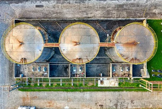
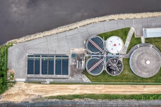
Hybrid Treatment System Blueprint: Process Flow, Removal Efficiencies, and Footprint
Achieving zero liquid discharge for semiconductors requires a robust, multi-stage hybrid treatment system designed to address the diverse and complex contaminant profiles of chip fab wastewater. A typical 600 GPM (gallons per minute) hybrid system blueprint, optimized for maximum water recovery and contaminant removal, integrates several advanced technologies in a sequential process:
- Equalization Tank: The process begins with a large equalization tank, providing a 24-hour retention time for flow and concentration buffering. This homogenizes the highly variable incoming wastewater streams, ensuring a stable feed for subsequent treatment stages.
- pH Adjustment: Following equalization, the wastewater undergoes precise pH adjustment, typically using an automatic chemical dosing system for PLC-controlled chemical dosing of caustic soda (e.g., 10% NaOH solution at 0.5–1.0 g/L) to optimize conditions for coagulation and precipitation, often raising pH to 7-9.
- Electrocoagulation (EC): This stage is critical for removing fluoride, heavy metals, and suspended solids from CMP and HF streams. Using sacrificial iron or aluminum electrodes, electrocoagulation achieves up to 95% fluoride removal and significant heavy metal precipitation. The EC unit for a 600 GPM plant would typically consume 0.5–1.0 kWh/m³ and have a retention time of 20–30 minutes.
- Dissolved Air Flotation (DAF): Post-EC, a high-performance ZSQ series DAF system for TSS removal in semiconductor wastewater is employed to efficiently separate the flocculated contaminants, oils, and finely suspended solids. DAF units typically achieve 97% TSS removal, generating a concentrated sludge float that is easier to dewater. For a 600 GPM system, the DAF unit might have a footprint of approximately 30–50 m² and consume 0.1–0.2 kWh/m³.
- Multi-Media Filtration (MMF) / Activated Carbon Filtration (ACF): After DAF, the clarified water passes through MMF to remove residual suspended solids (>5 micron) and then ACF to adsorb remaining organic compounds and trace contaminants, protecting downstream membrane systems.
- Reverse Osmosis (RO): The heart of the water recovery process, a high-recovery RO system for TDS removal in chip fab wastewater is used to remove dissolved salts, heavy metals, and other non-volatile contaminants. A two-stage RO system can achieve 95% TDS recovery, producing high-quality permeate suitable for reuse as process water or for further polishing to UPW standards. For a 600 GPM system, RO typically operates at 60–75% recovery per pass, with overall system recovery optimized through permeate recycling and brine concentration. Energy consumption ranges from 1.5–3.0 kWh/m³.
- Evaporation/Crystallization (ZLD): The concentrated brine from the RO system is then directed to an evaporator-crystallizer for final ZLD. This thermal process boils off the remaining water, leaving behind solid salts for disposal, ensuring virtually 100% water recovery from the concentrated stream. Evaporators are energy-intensive, consuming 20–40 kWh/m³ of brine, but are essential for complete zero liquid discharge.
This hybrid approach ensures high removal efficiencies across all critical parameters: Fluoride 95% (electrocoagulation), TSS 97% (DAF), TDS 95% (RO), and heavy metals 99% (ion exchange, if a polishing step is added after RO). The integrated design offers a significantly reduced footprint compared to conventional multi-component systems. A 600 GPM hybrid system can typically fit within a 1,200 m² footprint, whereas a conventional system with comparable capacity might require 2,500 m². For example, Saltworks' 600 GPM HF plant demonstrates a modular design achieving 99% water recovery with a reported 12-month ROI from water savings, highlighting the efficiency and economic benefits of such advanced systems. Further details on hybrid ZLD system designs for semiconductor wastewater can be found in our specialized articles.
ZLD System Costs: CAPEX, OPEX, and ROI for 2025 Chip Fabs
Implementing a zero-liquid-discharge (ZLD) system for semiconductor fabs represents a significant investment, but the long-term operational savings, regulatory compliance, and water security benefits often yield a compelling return on investment. The total cost of ownership for a ZLD system for 2025 chip fabs encompasses both capital expenditure (CAPEX) and operational expenditure (OPEX).
For a typical 600 GPM ZLD system, the CAPEX can range from $15–$25 million, broken down as follows:
- Electrocoagulation Unit: $1.2 million
- Dissolved Air Flotation (DAF) System: $800,000
- Reverse Osmosis (RO) System: $3.5 million
- Evaporation/Crystallization Unit: $5.0 million
- Civil Works, Piping, Instrumentation, Electrical: $2.5 million
- Engineering, Project Management, Commissioning: $2.0 million
- Contingency (10-15%): $1.5–$2.5 million
- Total Estimated CAPEX: $15–$25 million
Operational expenditure (OPEX) for ZLD systems typically ranges from $0.80–$1.50 per 1,000 gallons ($0.21–$0.40/m³) treated, with key components including:
- Energy Consumption: Approximately $0.50/m³ (primarily for RO and evaporation)
- Chemicals: Approximately $0.20/m³ (for pH adjustment, anti-scalants, coagulants)
- Labor: Approximately $0.10/m³ (for operation, maintenance, monitoring)
- Sludge/Solid Waste Disposal: Approximately $0.15/m³ (for hazardous sludge and crystallized salts)
- Maintenance & Spares: Approximately $0.10/m³
- Total Estimated OPEX: $0.80–$1.50 per 1,000 gallons treated
The return on investment (ROI) for advanced wastewater treatment systems is driven by several factors:
- Water Savings: Recycled water often costs $0.50/m³ to produce, significantly less than the $1.20/m³ or more for fresh municipal or well water, leading to substantial savings.
- Avoidance of Permit Fines: As exemplified by the Phoenix fab case, avoiding fines of $2.1 million per year for exceeding discharge limits provides a direct and immediate financial benefit.
- CHIPS Act Tax Credits: The CHIPS Act offers incentives, including potential tax credits that can cover up to 30% of eligible CAPEX, reducing the initial investment burden.
- Enhanced Brand Reputation & Sustainability: While harder to quantify, improved environmental performance can enhance corporate image and market value.
A notable case study involves a 2024 fab in Taiwan, where an $18 million ZLD system achieved payback in 3.2 years through a combination of significant water savings and government tax credits. This demonstrates the strong economic viability of ZLD systems when considering the total value proposition.
| Metric | ZLD System (Hybrid) | Conventional Treatment (Discharge) |
|---|---|---|
| CAPEX | $15–$25 Million | $5–$10 Million |
| OPEX (per 1,000 Gallons) | $0.80–$1.50 | $0.30–$0.70 |
| Footprint | 1,200–1,500 m² | 2,000–3,000 m² |
| Water Recovery Rate | 95%+ | 0–20% (for direct reuse) |
| Discharge Volume | Minimal (solid waste only) | High (liquid effluent) |
| Permit Violation Risk | Very Low | Moderate to High |
| CHIPS Act Eligibility | High (for U.S. fabs) | Low |
Selecting a Chip Fab Wastewater Treatment Vendor: 2025 Decision Framework
Choosing the right vendor for chip fab developer wastewater treatment is a strategic decision that impacts operational efficiency, compliance, and long-term costs. A structured, data-driven approach is essential for evaluating providers and ensuring the selected solution meets the stringent demands of semiconductor manufacturing. The following decision framework outlines key criteria for 2025 fab projects:
- Water Recovery Rate: Prioritize vendors demonstrating proven systems with a target recovery rate of 95% or higher, critical for water-scarce regions and ZLD compliance.
- System Footprint: Evaluate the physical space required. Modular, compact designs are preferable, with a target footprint of less than 1,500 m² for a 600 GPM plant to minimize valuable fab real estate.
- Operational Expenditure (OPEX): A detailed OPEX projection is crucial. Target vendors offering solutions with OPEX below $1.00/m³ (approx. $3.78/1,000 gallons) through energy-efficient processes and optimized chemical consumption.
- Modularity and Scalability: Favor vendors providing skid-mounted, modular systems that allow for rapid deployment, easier expansion, and reduced on-site construction time.
- Compliance Expertise: Verify the vendor's ability to meet and exceed current and anticipated regulatory standards, specifically China GB8978-2025 and U.S. EPA 40 CFR Part 469 for semiconductor manufacturing.
Red Flags to Watch For:
- No semiconductor-specific project references or case studies.
- Limited or no experience with zero-liquid-discharge (ZLD) systems.
- Reliance on proprietary chemicals or components that could lead to vendor lock-in and inflated long-term costs.
A recent 2023 vendor selection process for a fab in Singapore provides a practical example. The fab shortlisted three vendors based on initial proposals. Zhongsheng Environmental ultimately secured the contract by demonstrating a proven system with a 96% water recovery rate and a projected OPEX of $0.95/m³, alongside a modular design featuring advanced ZSQ series DAF systems and high-recovery RO systems. This outcome underscores the importance of a comprehensive evaluation that goes beyond initial CAPEX to consider total cost of ownership and performance guarantees.
| Criterion | Vendor A (e.g., Zhongsheng Environmental) | Vendor B (e.g., Saltworks) | Vendor C (e.g., IDE Tech) | Vendor D | Vendor E |
|---|---|---|---|---|---|
| Water Recovery Rate | 96%+ | 95%+ | 97%+ | 90% | 92% |
| Footprint (600 GPM) | ~1,200 m² (Modular) | ~1,300 m² (Modular) | ~1,100 m² (Modular) | ~2,000 m² (Conventional) | ~1,800 m² (Semi-modular) |
| OPEX (per m³) | ~$0.95 | ~$1.05 | ~$0.90 | ~$1.30 | ~$1.15 |
| Modularity | High (Skid-mounted) | High (Skid-mounted) | High (Skid-mounted) | Moderate (Some custom build) | Moderate (Some custom build) |
| Compliance Expertise | Excellent (Global) | Excellent (North America) | Excellent (Global) | Good (Regional) | Good (Regional) |
Frequently Asked Questions
Engineers and procurement teams evaluating wastewater treatment systems for semiconductor fabs often have specific technical and cost-related questions. Here are answers to some of the most common inquiries:
Q: What is the biggest challenge in treating chip fab wastewater?
A: The biggest challenge is managing rising total dissolved solids (TDS) concentrations due to continuous water recycling efforts within the fab. Conventional systems struggle with influent TDS levels exceeding 10,000 mg/L. To achieve 95%+ water recovery and meet stringent discharge or reuse requirements, advanced zero-liquid-discharge (ZLD) systems incorporating high-recovery reverse osmosis (RO) followed by evaporation and crystallization are typically required (Saltworks 2024 data).
Q: How much does a 600 GPM ZLD system cost for a chip fab?
A: For a 600 GPM chip fab ZLD system, the capital expenditure (CAPEX) generally ranges from $15–$25 million. Operational expenditure (OPEX) typically falls between $0.80–$1.50 per 1,000 gallons ($0.21–$0.40/m³) treated. The return on investment (ROI) is usually achieved within 3–5 years through significant water savings, avoidance of substantial permit fines, and eligibility for tax credits under initiatives like the CHIPS Act (2025 cost benchmarks).
Q: Can electrocoagulation remove fluoride from HF wastewater?
A: Yes, electrocoagulation with sacrificial iron electrodes is highly effective for hydrofluoric acid wastewater neutralization and fluoride removal. It can achieve up to 95% fluoride removal from influent concentrations ranging from 100–500 mg/L (Elsevier 2024). While effective, the disposal costs for the generated fluoride-containing sludge, which can be around $1,200 per ton, must be carefully factored into the overall OPEX calculations for the chip fab developer wastewater treatment system.
Q: What are the permit limits for arsenic in chip fab wastewater?
A: Permit limits for arsenic in chip fab wastewater are very stringent due to its toxicity. China's GB8978-2025 standard limits arsenic to 0.1 mg/L, while the U.S. EPA 40 CFR Part 469 sets an even lower limit of 0.05 mg/L. To meet these tight regulations, adsorption with granular ferric hydroxide (GFH) media or specialized ion exchange resins are the most effective removal methods, capable of achieving 99%+ efficiency.
Q: How do I reduce the footprint of a chip fab wastewater treatment system?
A: To reduce the physical footprint of a chip fab wastewater treatment system, prioritize modular, skid-mounted designs and integrate hybrid processes. For example, combining electrocoagulation with a compact ZSQ series DAF system can significantly reduce the space needed compared to conventional coagulation-sedimentation tanks. Utilizing vertical-stacking or compact high-recovery RO units also saves space. With an optimized modular design, a 600 GPM system can be engineered to fit within approximately 1,200 m², as demonstrated by successful projects like the Saltworks case study, minimizing civil works and allowing for rapid deployment.
Related Equipment
- ZSQ series DAF system for TSS removal in semiconductor wastewater — view specifications, capacity range, and technical data
- high-recovery RO system for TDS removal in chip fab wastewater — view specifications, capacity range, and technical data
- PLC-controlled chemical dosing for pH adjustment and coagulation — view specifications, capacity range, and technical data
Need a customized solution? Request a free quote with your specific flow rate and pollutant parameters.