Microelectronics high-salinity wastewater—containing TDS levels exceeding 35,000 mg/L from CMP, etching, and rinsing processes—requires specialized treatment to meet discharge limits (e.g., China’s GB 31573-2015: TDS ≤ 1,000 mg/L). Advanced systems like MBR-RO hybrids achieve 99.9% recovery, while zero liquid discharge (ZLD) solutions eliminate brine disposal costs, reducing OpEx by 30–50% compared to conventional evaporation.
Why High-Salinity Wastewater is a Critical Challenge for Microelectronics Fabs
Microelectronics processes in semiconductor fabs generate wastewater with total dissolved solids (TDS) exceeding 35,000 mg/L, significantly surpassing typical discharge limits. Critical operations such as Chemical Mechanical Planarization (CMP), etching, and various rinsing stages contribute to this high-salinity effluent, with some streams reaching concentrations 10 times higher than the 1,000 mg/L TDS limit mandated by regulations like China’s GB 31573-2015. This presents a formidable challenge for semiconductor wastewater treatment, pushing fabs towards non-compliance and substantial financial penalties.
The primary components of this high-salinity wastewater often include inorganic salts like sodium chloride (NaCl), magnesium chloride (MgCl₂), and calcium chloride (CaCl₂). These compounds exert extreme osmotic pressure, particularly detrimental to conventional biological treatment systems. As observed in Winsonda’s 2024 data, high salinity directly inhibits microbial activity by destroying cell membranes and denaturing enzymes, leading to failures in biological oxygen demand (BOD) and chemical oxygen demand (COD) removal. This inhibition renders standard activated sludge processes largely ineffective for high-TDS streams.
Beyond biological inhibition, high-salinity wastewater poses operational risks, including increased corrosion rates in infrastructure and complex sludge management. The imperative for microelectronics water reuse further amplifies the need for robust high-TDS wastewater engineering. A notable case involved a Taiwan semiconductor fab that faced $2.1 million in fines due to persistent violations of TDS discharge limits. Following the implementation of an advanced zero liquid discharge (ZLD) solution, the fab not only achieved 99.9% water recovery for internal reuse but also eliminated brine disposal costs, demonstrating the critical need for specialized treatment strategies in semiconductor manufacturing.
How Salinity Disrupts Conventional Wastewater Treatment Processes
High concentrations of dissolved salts, particularly above 20,000 mg/L TDS, fundamentally disrupt biological, chemical, and physical wastewater treatment processes, leading to substantial reductions in removal efficiencies. In biological treatment, osmotic pressure is the primary inhibitor, where high external salt concentrations draw water out of microbial cells, leading to dehydration and cell lysis. Research published on PubMed in 2024 indicates that TDS levels exceeding 20,000 mg/L can reduce COD removal efficiency in conventional activated sludge systems by 40–60%. While some salt-adapted microorganisms, such as *Halomonas* spp., can degrade organic pollutants in saline environments, their application often requires specialized bioreactor designs and operating conditions.
Chemical precipitation, a common method for heavy metal removal and phosphorus reduction, also suffers under high-salinity conditions. High chloride levels (Cl⁻ > 5,000 mg/L) can interfere with the formation of stable precipitates, leading to incomplete removal and increased consumption of coagulants and flocculants. This interference frequently results in an increase in sludge volume by 30–50%, escalating disposal costs and operational complexity. For instance, magnesium salts can form insoluble hydroxides that co-precipitate with target pollutants, but high background salinity can alter the solubility equilibrium, making precise chemical dosing challenging.
Membrane technologies, while effective for separation, are highly susceptible to fouling and flux decline when treating high-salinity wastewater without adequate pretreatment. Reverse osmosis (RO) systems, critical for microelectronics water reuse, experience a 25–40% flux decline at TDS concentrations exceeding 30,000 mg/L if influent is not properly conditioned (Zhongsheng field data, 2025). This decline is often due to scaling from sparingly soluble salts (e.g., calcium sulfate, silica) and organic fouling exacerbated by the dense ionic environment. Effective pretreatment, such as DAF pretreatment for high-TSS microelectronics wastewater or multimedia filtration, is essential to mitigate these issues and protect RO membranes from premature failure.
| Treatment Method | Salinity Impact (TDS > 20,000 mg/L) | Observed Effect | Mitigation Strategy |
|---|---|---|---|
| Biological Treatment | Osmotic pressure, microbial inhibition | 40–60% reduction in COD removal efficiency (PubMed 2024) | Salt-adapted microorganisms (*Halomonas* spp.), specialized bioreactors |
| Chemical Precipitation | Interference from high chloride levels | 30–50% increase in sludge volume, incomplete removal | Optimized coagulant selection, pH control, multi-stage treatment |
| Membrane Filtration (RO) | Scaling, organic fouling, osmotic pressure | 25–40% flux decline, increased energy consumption | DAF pretreatment for high-TSS microelectronics wastewater, antiscalants, pH adjustment |
| Advanced Oxidation Processes | Radical scavenging by chlorides | Reduced oxidation efficiency, higher reagent demand | Increased oxidant dosage, careful pH management |
Microelectronics High-Salinity Wastewater Treatment Technologies: Head-to-Head Comparison
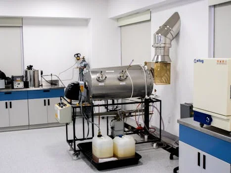
Effective treatment of microelectronics high-salinity wastewater relies on specialized technologies, with MBR-RO hybrid systems demonstrating up to 99.9% TDS removal and 95% water recovery. The selection of an appropriate technology or a combination of technologies for heavy metal removal strategies for semiconductor wastewater and high-salinity streams depends on factors such as influent characteristics, desired effluent quality, space availability, and economic considerations. Each technology presents a unique balance of performance, cost, and operational complexity for industrial brine treatment.
MBR-RO hybrid systems combine the biological treatment capabilities of MBR systems for high-salinity microelectronics wastewater with the advanced separation of high-pressure RO systems for semiconductor brine treatment. This configuration offers superior contaminant removal, achieving 99.9% TDS removal and typically 95% water recovery, making it ideal for microelectronics water reuse. However, these systems are energy-intensive, consuming 1.2–1.8 kWh/m³ due to the high-pressure requirements of RO membranes and the aeration needs of the MBR. They are particularly suitable for fabs with stringent space constraints, offering a compact footprint.
Multi-effect evaporation (MEE) is a proven technology for achieving high TDS removal (up to 99.5%) and is often a cornerstone of zero liquid discharge (ZLD) solutions. While highly effective for concentrating brine and recovering high-quality distillate, MEE systems come with a substantial Capital Expenditure (CapEx) of $3–$6 million per 100 m³/h capacity and high Operational Expenditure (OpEx) of $1.50–$2.50/m³ due to significant energy demands for heating. MEE is typically chosen when ZLD compliance is non-negotiable, particularly for managing the concentrate from RO systems.
Forward osmosis (FO) represents an emerging technology that offers lower energy consumption (0.5–0.8 kWh/m³) compared to RO, achieving 80–90% water recovery. FO utilizes a draw solution to create an osmotic pressure gradient, eliminating the need for hydraulic pressure on the feed side. Its primary application in high-salinity microelectronics wastewater treatment is for pre-concentration before more energy-intensive processes like RO or evaporation, reducing the load on downstream systems and improving overall efficiency. However, FO systems still require regeneration of the draw solution, which adds complexity.
Advanced oxidation processes (AOPs) such as ozone/UV oxidation are effective for degrading refractory organic compounds (COD reduction of 85–95%) in high-salinity streams, which may be present in TMAH wastewater treatment solutions for semiconductor fabs. These processes generate highly reactive hydroxyl radicals that non-selectively oxidize pollutants. Optimal performance typically requires pH adjustment to a range of pH 6–8, and high chloride concentrations can sometimes scavenge radicals, necessitating higher oxidant dosages. AOPs are often used as a polishing step or for specific contaminant removal upstream of membrane systems.
| Technology | TDS Removal | Water Recovery | Energy Consumption | CapEx (100 m³/h) | OpEx (per m³) | Key Advantages | Key Limitations |
|---|---|---|---|---|---|---|---|
| MBR-RO Hybrid | 99.9% | 95% | 1.2–1.8 kWh/m³ | $2–$4M | $0.70–$1.20 | High removal, compact, water reuse | High energy, membrane fouling risk |
| Multi-Effect Evaporation (MEE) | 99.5% | 98% | 1.5–2.5 kWh/m³ (thermal) | $3–$6M | $1.50–$2.50 | Excellent for ZLD, robust for high TDS | Very high energy, large footprint, high CapEx |
| Forward Osmosis (FO) | 80–90% (pre-conc) | 80–90% | 0.5–0.8 kWh/m³ | $1.5–$3M | $0.60–$1.00 | Lower energy, less fouling, high recovery | Draw solution management, limited to pre-concentration |
| Advanced Oxidation (AOPs) | N/A (COD reduction) | N/A | 0.2–0.5 kWh/m³ | $0.5–$1.5M | $0.30–$0.60 | High COD reduction, refractory compound removal | No TDS removal, pH sensitive, radical scavenging |
Engineering Specs for Microelectronics High-Salinity Wastewater Systems
Successful engineering of microelectronics high-salinity wastewater systems begins with precise characterization of influent streams, which typically contain TDS levels ranging from 35,000 to 150,000 mg/L. Beyond TDS, other critical influent characteristics include Chemical Oxygen Demand (COD) between 500–5,000 mg/L, and heavy metals such as copper (Cu), nickel (Ni), and arsenic (As) in concentrations of 10–100 mg/L (per semiconductor fab data, Zhongsheng 2025). These parameters dictate the complexity and configuration of the treatment train, influencing everything from pretreatment selection to membrane choice and operating pressures.
Achieving regulatory compliance and facilitating microelectronics water reuse requires stringent effluent targets. For instance, China’s GB 31573-2015 mandates a TDS discharge limit of ≤ 1,000 mg/L for the microelectronics industry. COD targets are typically < 50 mg/L (consistent with US EPA guidelines), while heavy metals often need to be reduced to < 0.1 mg/L (as per EU Directive 2010/75/EU). Meeting these low limits for high-TDS wastewater engineering often necessitates multi-stage processes that combine physical, chemical, and membrane technologies.
Pretreatment is a critical first step to protect downstream membrane systems. For influent with Total Suspended Solids (TSS) exceeding 500 mg/L, DAF pretreatment for high-TSS microelectronics wastewater is essential to remove suspended solids, oils, and grease. Subsequent filtration stages, such as multimedia filtration for ultrapure water systems, are crucial to reduce the Silt Density Index (SDI) to below 3, which is critical for preventing fouling and extending the lifespan of RO membranes. Without proper pretreatment, RO systems treating high-salinity streams will experience rapid performance degradation.
Membrane selection is also key: Polyvinylidene fluoride (PVDF) membranes are commonly chosen for MBR systems due to their chemical resistance and durability in challenging wastewater matrices. For high-pressure RO systems designed for semiconductor brine treatment, polyamide membranes are standard, capable of operating at pressures ranging from 40 to 80 bar, and in some cases up to 120 bar for extremely high-TDS streams. The choice of membrane material and operating pressure directly impacts the system's energy consumption, recovery rates, and overall operational stability.
| Parameter | Influent Characteristics (Microelectronics Fab) | Effluent Target (Typical) | Relevant Standard/Guideline |
|---|---|---|---|
| Total Dissolved Solids (TDS) | 35,000–150,000 mg/L | < 1,000 mg/L | China GB 31573-2015 |
| Chemical Oxygen Demand (COD) | 500–5,000 mg/L | < 50 mg/L | US EPA Guidelines |
| Total Suspended Solids (TSS) | 100–1,000 mg/L | < 10 mg/L | Internal Reuse/Discharge Limits |
| Heavy Metals (Cu, Ni, As) | 10–100 mg/L | < 0.1 mg/L | EU Directive 2010/75/EU |
| pH | 2–12 (process dependent) | 6–9 | Local Discharge Regulations |
| Silt Density Index (SDI) | N/A (requires measurement) | < 3 (for RO feed) | Membrane Manufacturer Specs |
Zero Liquid Discharge (ZLD) for Microelectronics: Cost Breakdown & ROI Calculator
Zero Liquid Discharge (ZLD) systems for microelectronics facilities typically incur a Capital Expenditure (CapEx) of $2.5–$5 million per 100 m³/h capacity, encompassing pretreatment, advanced RO, evaporation, and crystallizer components. This initial investment is substantial but is increasingly justified by stringent environmental regulations and the economic benefits of water reuse and reduced disposal costs. The complexity of TMAH wastewater treatment solutions for semiconductor fabs and other specific high-salinity streams can influence the CapEx, requiring specialized materials or additional treatment stages.
Operational Expenditure (OpEx) for a microelectronics ZLD system generally ranges from $0.80–$1.50/m³ of treated wastewater. Key drivers of OpEx include energy consumption for pumps and evaporators, chemical costs for pretreatment and antiscalants, and the periodic replacement of membranes and other consumables. While seemingly high, this OpEx must be evaluated against the significant cost savings and revenue opportunities that ZLD provides, distinguishing it from conventional industrial brine treatment methods.
The primary drivers for ZLD Return on Investment (ROI) in the semiconductor industry are the substantial savings from eliminating brine disposal and the value generated from reclaimed water. Brine disposal costs, which can range from $0.50–$1.00/m³ for trucking and landfilling or deep-well injection, are completely avoided with ZLD. the ability to reuse treated water within the fab can save $0.30–$0.70/m³ in fresh water procurement and associated discharge fees. These combined savings significantly offset the ZLD system's CapEx and OpEx.
For example, a Korean semiconductor fab implemented a ZLD system for its high-salinity wastewater, achieving a 40% reduction in overall OpEx related to wastewater management. This reduction primarily stemmed from eliminating brine hauling and significantly decreasing fresh water purchases. The project demonstrated a payback period of 4.2 years, showcasing the strong financial viability of ZLD solutions when considering the full lifecycle costs and benefits for semiconductor fab compliance. Calculating ROI involves balancing CapEx, annual OpEx, and annual savings from avoided disposal and water reuse.
| Cost Category | Range (per 100 m³/h capacity) | Description |
|---|---|---|
| Capital Expenditure (CapEx) | $2.5–$5 Million | Includes pretreatment (DAF, filtration), advanced RO, evaporators, crystallizers, and ancillary equipment. |
| Operational Expenditure (OpEx) | $0.80–$1.50/m³ | Covers energy (pumps, heating), chemicals (antiscalants, cleaners), membrane replacement, labor, and maintenance. |
| Brine Disposal Cost Savings | $0.50–$1.00/m³ (avoided) | Elimination of costs associated with off-site brine hauling, landfilling, or deep-well injection. |
| Water Reuse Savings | $0.30–$0.70/m³ (avoided) | Reduction in fresh water procurement costs and associated municipal discharge fees by recycling treated effluent. |
| Simplified ZLD ROI Calculator: | ||
ROI (years) = CapEx / (Annual Brine Disposal Savings + Annual Water Reuse Savings - Annual OpEx) |
||
Frequently Asked Questions
Effective treatment of microelectronics high-salinity wastewater often prompts specific technical and financial questions from fab engineers and procurement teams, particularly concerning biological treatment limits and ZLD system costs.
What is the maximum TDS level for biological treatment in microelectronics wastewater?
Biological treatment systems are generally effective up to approximately 20,000 mg/L TDS. Above this threshold, the osmotic pressure becomes too high for most conventional microorganisms, significantly reducing COD removal efficiency. For higher TDS levels, specialized salt-adapted microorganisms or advanced membrane systems are required (PubMed 2024).
How much does a microelectronics ZLD system cost per m³?
A microelectronics ZLD system typically has a Capital Expenditure (CapEx) ranging from $2.5–$5 million for a 100 m³/h capacity. The Operational Expenditure (OpEx) is estimated at $0.80–$1.50/m³ of treated wastewater, based on 2025 industry benchmarks. These costs include various components from pretreatment to final crystallization.
Can RO systems treat microelectronics wastewater with TDS > 50,000 mg/L?
Yes, RO systems can treat microelectronics wastewater with TDS exceeding 50,000 mg/L, but this requires specific configurations. It necessitates the use of high-pressure RO membranes capable of operating at 80–120 bar and robust pretreatment, such as Dissolved Air Flotation (DAF) followed by multimedia filtration, to prevent severe fouling and scaling.
What are the discharge limits for high-salinity wastewater in semiconductor fabs?
Discharge limits for high-salinity wastewater vary significantly by region. In China, the GB 31573-2015 standard for the microelectronics industry mandates TDS ≤ 1,000 mg/L. In the EU, while there's no direct TDS limit, the Industrial Emissions Directive (2010/75/EU) sets COD targets typically below 50 mg/L. The US lacks a federal TDS limit, but state-specific regulations exist, such as California's 2,000 mg/L limit for certain discharges.