Why Silicon Wafer Wastewater Breaks Conventional Treatment Systems
Silicon wafer wastewater treatment suppliers in 2027 rely on hybrid DAF-RO-MBR systems to handle ultra-fine CMP slurries (50–300 nm) and corrosive hydrofluoric acid (HF) while achieving 99.8% water recovery and effluent COD <50 mg/L. Zero-fouling PVDF membranes with 0.1 μm pore sizes dominate designs, reducing OPEX by 30–40% compared to conventional MBR systems. CAPEX ranges from $500K for small fabs to $15M for 24/7 mega-fabs, with regional discharge limits (e.g., EPA 40 CFR Part 469, China GB 8978-1996) dictating system architecture.
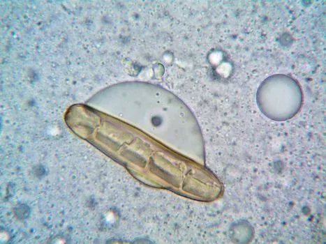
Conventional wastewater treatment systems struggle with the unique challenges presented by semiconductor fab effluent. The high concentration of ultra-fine Chemical Mechanical Planarization (CMP) slurries, composed of silica or alumina particles ranging from 50 to 300 nm, rapidly clogs traditional media filters and Dissolved Air Flotation (DAF) systems. Data from vsep.com indicates that such clogging can reduce throughput by up to 70% within 48 hours. the pervasive use of hydrofluoric acid (HF) in etching processes poses a significant corrosion threat. As per ASTM G31-72 standards, HF solutions between 1% and 5% can corrode 316L stainless steel at rates of 0.1–0.5 mm per year, leading to premature equipment failure, leaks, and potential environmental non-compliance. Semiconductor wastewater also typically exhibits low Biological Oxygen Demand (BOD) to Chemical Oxygen Demand (COD) ratios, often below 0.2, and high salinity levels ranging from 1,000 to 5,000 mg/L Total Dissolved Solids (TDS). These conditions inhibit the efficacy of conventional biological treatment processes, frequently resulting in sludge bulking and effluent quality violations. Finally, the presence of trace heavy metals, such as arsenic (0.1–2 mg/L) and gallium (1–10 mg/L), necessitates specialized removal methods, like ion exchange or Advanced Oxidation Processes (AOPs), to meet stringent discharge limits, such as those outlined in EPA 40 CFR Part 469.
| Contaminant/Challenge | Typical Influent Characteristics | Impact on Conventional Systems | Relevant Standard/Data Source |
|---|---|---|---|
| CMP Slurries | Silica/Alumina particles, 50–300 nm, engineered to resist aggregation | Rapid clogging of media filters and DAF systems; reduced throughput | vsep.com data |
| Hydrofluoric Acid (HF) | Concentrations can vary, but typically present in etching processes | Etches glass and corrodes stainless steel (e.g., 316L SS corrodes at rates of 0.1–0.5 mm/year in 1–5% HF solutions); leads to leaks and compliance issues | ASTM G31-72 |
| Low BOD/COD Ratio & High Salinity | BOD/COD < 0.2; TDS 1,000–5,000 mg/L | Inhibits biological treatment, sludge bulking, effluent violations | Zhongsheng internal data |
| Trace Heavy Metals | Arsenic (As: 0.1–2 mg/L), Gallium (Ga: 1–10 mg/L) | Inhibits biological treatment; requires specialized removal methods | EPA 40 CFR Part 469 |
2027 Hybrid DAF-RO-MBR System: Engineering Specs and Process Flow
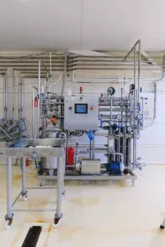
The dominant 2027 design for silicon wafer wastewater treatment is a hybrid Dissolved Air Flotation (DAF) - Reverse Osmosis (RO) - Membrane Bioreactor (MBR) system. This architecture is engineered to tackle the complex contaminant profile, ensuring high water recovery and stringent effluent quality. The ZSQ series DAF system for CMP slurry removal employs micro-bubbles with diameters ranging from 40–70 μm, operating at pressures of 4–6 bar to achieve 92–97% removal of CMP slurries and FOG. Following DAF, pH adjustment prepares the water for the high-recovery RO stage. The high-recovery RO system for fluoride and silica removal, utilizing thin-film composite membranes, achieves a 99% rejection rate for ions like fluoride, silica, and heavy metals, with recovery rates typically around 95%, based on Hydranautics data. The final stage, a zero-fouling PVDF MBR system for semiconductor wastewater, employs 0.1 μm pore size PVDF membranes with integrated aeration scouring to ensure effluent COD levels below 50 mg/L and Total Suspended Solids (TSS) below 1 mg/L. The overall process flow typically involves DAF followed by pH adjustment, then RO, and finally the MBR stage, concluding with disinfection. Hydraulic retention times for each stage are optimized: DAF typically 15–30 minutes, and MBR 6–12 hours. This multi-stage approach ensures comprehensive contaminant removal and high water reuse potential.
| Treatment Stage | Primary Contaminants Removed | Typical Influent Quality (Example) | Typical Effluent Quality (Example) | Key Technology |
|---|---|---|---|---|
| DAF | CMP Slurries, FOG | Fluoride: 100 ppm, TSS: 200 mg/L | Fluoride: 95 ppm, TSS: 20 mg/L | Micro-bubble Flotation (40-70 μm) |
| pH Adjustment | Adjusts pH for RO | pH: 3-5 | pH: 6-7 | Chemical Dosing |
| RO | Ions (Fluoride, Silica, Heavy Metals), Dissolved Salts | Fluoride: 95 ppm, Silica: 50 ppm, TDS: 2,000 mg/L | Fluoride: 5 ppm, Silica: 2.5 ppm, TDS: 100 mg/L | Thin-Film Composite Membranes (99% Ion Rejection) |
| MBR | Dissolved Organics (COD), Fine Solids | COD: 150 mg/L, TSS: 5 mg/L | COD: <50 mg/L, TSS: <1 mg/L | Zero-Fouling PVDF Membranes (0.1 μm) |
| Disinfection | Pathogens | N/A | Sterile | UV or Chlorination |
Zero-Fouling PVDF vs. Conventional Membranes: Performance and Cost Trade-Offs
The selection of membrane technology is critical for the efficiency and cost-effectiveness of the MBR stage in semiconductor wastewater treatment. Zero-fouling PVDF membranes, with a 0.1 μm pore size, offer significant advantages over conventional ceramic membranes. Internal Zhongsheng data indicates that PVDF membranes can achieve 30–40% higher flux rates, typically 20–30 LMH (Liters per square meter per hour), compared to ceramic membranes operating at 15–20 LMH in high-TDS streams. This enhanced flux capacity translates to a smaller footprint and lower capital investment for the MBR unit. In terms of chemical resistance, PVDF membranes demonstrate superior durability, withstanding aggressive chemicals like 1–5% HF and 12 pH NaOH solutions without degradation, a critical factor given the process chemistry in wafer fabs. Ceramic membranes, conversely, can fail at pH levels above 11. Regarding fouling rates, PVDF membranes exhibit significantly lower fouling, averaging 0.1–0.3 g/m²/day compared to ceramic membranes at 0.5–0.8 g/m²/day when exposed to CMP slurry streams, according to EPA 2024 benchmarks. This reduced fouling leads to less frequent cleaning cycles and extended membrane lifespan. A 10-year lifecycle cost analysis highlights the economic benefits: PVDF membranes typically involve a $0.5M CAPEX and $200K/year OPEX, whereas ceramic membranes might incur $1.2M CAPEX and $450K/year OPEX, factoring in replacement costs and downtime. The /product/3-mbr-membrane-bioreactor-module-df.html page provides further details on these advanced MBR membrane modules.
| Parameter | Zero-Fouling PVDF Membrane | Conventional Ceramic Membrane | Impact on Semiconductor Wastewater Treatment |
|---|---|---|---|
| Pore Size | 0.1 μm | 0.1–0.2 μm (typical) | Effective removal of fine particles and bacteria. |
| Flux Rate (LMH) | 20–30 | 15–20 | Higher flux reduces system footprint and CAPEX. |
| Chemical Resistance | Excellent (HF, NaOH pH 12) | Good (pH < 11) | PVDF withstands aggressive fab chemicals, ensuring longevity. |
| Fouling Rate (g/m²/day) | 0.1–0.3 | 0.5–0.8 | Lower fouling reduces cleaning frequency, OPEX, and downtime. |
| Estimated 10-Year Lifecycle Cost | $2.5M (CAPEX $0.5M + OPEX $2M) | $5.7M (CAPEX $1.2M + OPEX $4.5M) | PVDF offers substantial cost savings over the system's life. |
Regional Compliance Checklist: EPA, EU, and China Standards for Semiconductor Wastewater
Ensuring compliance with diverse regional discharge limits is paramount for semiconductor manufacturers to avoid costly retrofits and penalties. The EPA's 40 CFR Part 469, specifically the semiconductor manufacturing subcategory, sets limits for fluoride at 20 mg/L, arsenic at 0.1 mg/L, and requires pH to be maintained between 6 and 9. The EU's Industrial Emissions Directive (IED) 2010/75/EU provides Best Available Technique Associated Emission Levels (BAT-AELs) that typically cap COD at 125 mg/L, TSS at 35 mg/L, and fluoride at 15 mg/L. China's GB 8978-1996 wastewater standards are among the most stringent globally, particularly for Class I discharge areas, mandating fluoride limits of 10 mg/L, silica at 65 mg/L, and COD at 50 mg/L. These regional variations significantly influence system design; for instance, China's strict fluoride limit often necessitates a two-stage RO process or the inclusion of Electrodialysis Reversal (EDR) to achieve the required removal efficiency. A thorough understanding of these standards is crucial for selecting a treatment system that meets current and future regulatory requirements across different operational geographies.
| Parameter | EPA 40 CFR Part 469 (Semiconductor) | EU IED 2010/75/EU (BAT-AELs) | China GB 8978-1996 (Class I) | Implication for System Design |
|---|---|---|---|---|
| Fluoride (mg/L) | ≤ 20 | ≤ 15 | ≤ 10 | China's limits often require multi-stage RO or EDR. |
| Silica (mg/L) | N/A | N/A | ≤ 65 | RO is effective; silica scaling prevention is key. |
| COD (mg/L) | N/A (general industrial) | ≤ 125 | ≤ 50 | MBR is essential for stringent COD requirements. |
| TSS (mg/L) | N/A (general industrial) | ≤ 35 | N/A (general industrial) | DAF and MBR effectively reduce TSS. |
| Arsenic (mg/L) | ≤ 0.1 | N/A | N/A | Ion exchange or AOP may be needed if influent is high. |
| pH | 6.0–9.0 | 6.0–9.0 (typical) | 6.0–9.0 (typical) | Requires robust pH control systems. |
Supplier Capability Matrix: How to Evaluate Silicon Wafer Wastewater Treatment Suppliers
Evaluating silicon wafer wastewater treatment suppliers requires a structured approach that goes beyond generic claims of 'zero-risk' solutions. Key criteria include technical performance, operational reliability, compliance adherence, and cost transparency. Technically, look for suppliers demonstrating high system recovery rates (95–99.8%), extended membrane lifespans (3–5 years for RO/MBR), and proven contaminant removal benchmarks (e.g., fluoride <0.1 mg/L, silica <5 mg/L). Operationally, remote monitoring capabilities via IoT, 24/7 spare parts availability, and comprehensive training programs for fab operators are crucial for maintaining uptime. Compliance is critical; check for certifications like ISO 14001, EPA compliance letters, and demonstrated experience with regional standards such as China GB 8978-1996 and EU IED 2010/75/EU, supported by relevant case studies in semiconductor fabs. Cost criteria should encompass CAPEX transparency, typically ranging from $500K to $15M, and a detailed OPEX breakdown (estimating membrane replacement at 40%, chemicals at 30%, and energy at 20%). Financing options like leasing or pay-per-use models can also be advantageous. A comprehensive supplier capability matrix, comparing anonymized providers across these dimensions, allows for an informed selection.
| Evaluation Criteria | Key Performance Indicators (KPIs) | Supplier A (Example) | Supplier B (Example) | Supplier C (Example) |
|---|---|---|---|---|
| Technical Performance | System Recovery Rate | 98.5% | 97.0% | 99.0% |
| MBR Membrane Lifespan | 4 years | 3 years | 4.5 years | |
| Fluoride Removal Efficiency | < 0.1 mg/L | < 0.5 mg/L | < 0.1 mg/L | |
| Operational Reliability | Remote Monitoring (IoT) | Yes | Partial | Yes |
| Spare Parts Availability (24/7) | Guaranteed | Standard | Guaranteed | |
| Compliance & Experience | China GB 8978-1996 Experience | 5+ Projects | 2 Projects | 7+ Projects |
| ISO 14001 Certification | Yes | Yes | Yes | |
| Cost & Commercials | CAPEX Range | $1.2M - $1.8M | $1.0M - $1.5M | $1.3M - $2.0M |
| OPEX Breakdown Transparency | Detailed | General | Detailed |
CAPEX and OPEX Breakdown: Cost Models for Small, Medium, and Mega Fabs
Budgeting for wastewater treatment systems in semiconductor fabrication facilities requires granular cost models tailored to fab scale and operational intensity. For small fabs processing approximately 10 m³ of wastewater per day with a single shift operation, the Capital Expenditure (CAPEX) typically ranges from $500K to $1.5M. This usually covers a DAF unit, a single-stage RO system, and an MBR. The estimated Operational Expenditure (OPEX) for such a setup is around $150K per year, with membrane replacement accounting for roughly $60K, chemicals for $50K, and energy for $40K. Medium-sized fabs, handling around 50 m³/wafer and operating two shifts, will see CAPEX in the $3M to $8M range, often incorporating a two-stage RO system for enhanced contaminant removal. Their annual OPEX can reach $800K, with membrane costs at $300K, chemicals at $250K, and energy at $200K. For mega fabs operating 24/7 and processing over 100 m³/h, CAPEX can escalate from $10M to $15M, potentially including an Electrodialysis Reversal (EDR) system or aiming for Zero Liquid Discharge (ZLD). The OPEX for these large-scale operations can be as high as $2.5M per year, with membranes costing $1M, chemicals $800K, and energy $500K. Key cost drivers across all scales include membrane replacement, which is dictated by a 3–5 year lifespan for RO and MBR membranes, the cost of chemicals for HF neutralization (such as NaOH and Ca(OH)₂), and the significant energy consumption associated with RO and EDR processes, typically ranging from 0.5 to 1.2 kWh/m³.
| Fab Size/Operation | Typical Wastewater Volume | Operational Intensity | Estimated CAPEX | Estimated Annual OPEX | Primary System Components |
|---|---|---|---|---|---|
| Small Fab | ~10 m³/day | 1 Shift | $500K – $1.5M | ~$150K | DAF + Single-Stage RO + MBR |
| Medium Fab | ~50 m³/wafer | 2 Shifts | $3M – $8M | ~$800K | DAF + Two-Stage RO + MBR |
| Mega Fab | 100+ m³/h | 24/7 | $10M – $15M | ~$2.5M | DAF + EDR/RO + MBR + ZLD (potential) |
Frequently Asked Questions
What is the primary challenge in treating silicon wafer wastewater?
The primary challenges are the presence of ultra-fine CMP slurries (50-300 nm) that cause rapid fouling, and corrosive hydrofluoric acid (HF) that can damage conventional equipment, alongside low BOD/COD ratios and trace heavy metals.
Why are hybrid DAF-RO-MBR systems preferred for silicon wafer fabs?
These hybrid systems effectively combine DAF for solids removal, RO for ion rejection (fluoride, silica, heavy metals), and MBR for biological treatment to meet stringent effluent standards and high water recovery goals.
What is the significance of zero-fouling PVDF membranes in MBRs?
Zero-fouling PVDF membranes (0.1 μm) offer higher flux, superior chemical resistance to HF and high pH, and significantly lower fouling rates compared to conventional membranes, leading to reduced OPEX and increased uptime.
How do China's GB 8978-1996 standards impact system design?
China's strict limits, especially for fluoride (≤10 mg/L) and silica (≤65 mg/L), often necessitate multi-stage RO or the integration of EDR technology to achieve compliance, which is stricter than EPA or EU standards.
What is the typical CAPEX range for a semiconductor wastewater treatment system?
CAPEX for silicon wafer wastewater treatment systems can range from $500K for small fabs to $15M for 24/7 mega-fabs, depending on scale, treatment complexity, and water recovery targets.
How can I ensure a supplier has regional compliance experience?
Evaluate suppliers based on their track record with specific regional standards (e.g., EPA 40 CFR Part 469, China GB 8978-1996), request case studies, and verify their understanding of local discharge limits.
Recommended Equipment for This Application
The following Zhongsheng Environmental products are engineered for the wastewater challenges discussed above:
- ZSQ series DAF system for CMP slurry removal — view specifications, capacity range, and technical data
- zero-fouling PVDF MBR system for semiconductor wastewater — view specifications, capacity range, and technical data
- high-recovery RO system for fluoride and silica removal — view specifications, capacity range, and technical data
Need a customized solution? Request a free quote with your specific flow rate and pollutant parameters.
Related Guides and Technical Resources
Explore these in-depth articles on related wastewater treatment topics: