GaN semiconductor wastewater treatment CAPEX spans $2M for a 50 m³/h PVDF MBR to $40M–$50M for 1,000 m³/h ZLD plants. Influent loads run COD 500–3,000 mg/L and TSS 200–1,500 mg/L (3–5× silicon), with Ga, Al, and As often above permit limits.
Why GaN Wastewater Treatment Differs From Silicon Fab Streams
GaN fab effluent carries COD of 500–3,000 mg/L and TSS of 200–1,500 mg/L—about 3–5× silicon loads—plus dissolved Ga, Al, and As that generic industrial permits rarely anticipate. Equalization, metals precipitation, and robust membrane materials are therefore mandatory, not optional, on SiC or PVDF trains at 50–1,000 m³/h that commonly budget $2M–$50M CAPEX from MBR-only to ZLD.
GaN fabrication processes generate 3–5× higher COD and TSS than traditional silicon manufacturing. Per 2026 SEMATECH data cited in plant design packages, GaN effluent COD sits between 500–3,000 mg/L and TSS between 200–1,500 mg/L because of gallium etching chemistries and nitride byproducts. Those loads foul conventional membranes faster and overwhelm biological systems sized for lighter industrial streams. For the permeate numbers an MBR stage can actually hold, see our MBR Effluent Quality: Specs, Removal Rates and Selection Guide.
The chemistry behind those loads is distinctive. GaN is a wide-bandgap semiconductor grown by metal-organic vapour phase epitaxy, using ammonia with trimethylgallium or triethylgallium as precursors at growth temperatures between 800 and 1100 °C, typically deposited on sapphire or silicon carbide and increasingly on standard silicon wafers (Wikipedia, Gallium nitride). GaN dust is an irritant to skin, eyes and lungs, and rinse water from epitaxy tools carries metalorganics and nitride fines that behave nothing like silicon oxide slurries.
Beyond organics, GaN wastewater carries trace metals such as gallium (Ga), aluminum (Al), and arsenic (As). Gallium often exceeds EPA 40 CFR Part 469 limits of <1.0 mg/L, aluminum <0.2 mg/L, and arsenic <0.1 mg/L as those numbers circulate in fab design packages. Emerging EU and China standards are stricter still, often requiring 0.5 mg/L for Ga and 0.05 mg/L for As. Hydrolysis of gallium chloride (GaCl₃) forms insoluble gallium hydroxides; nitride compounds precipitate; and 50–80°C temperature swings age polymeric membranes faster than silicon rinse water at 20–50°C.
Arsenic deserves one scoping note. Arsenic belongs to GaN-adjacent chemistries such as gallium arsenide, so As limits usually bind on mixed III-V campuses that also run GaAs lines rather than on pure GaN-on-silicon tools. Confirm which tools feed the sewer before paying for arsenic-grade polishing on a GaN-only line.
| Parameter | GaN Wastewater | Silicon Wastewater |
|---|---|---|
| COD (mg/L) | 500–3,000 | 100–500 |
| TSS (mg/L) | 200–1,500 | 50–200 |
| Gallium (Ga) (mg/L) | Trace–5.0+ | N/A |
| Aluminum (Al) (mg/L) | Trace–3.0+ | Trace–1.0 |
| Arsenic (As) (mg/L) | Trace–0.5+ | N/A |
| pH Range | 1–13 (variable) | 4–10 |
| Temperature (°C) | 50–80 | 20–50 |
How Do You Design for Variable Fab Chemistry?
GaN Fab MBR System Design in 2027: Equalization and Dump Segregation
Semiconductor wastewater treatment system design for variable chemistry starts with equalization and metal speciation control before any membrane stage. Most GaN lines we size see pH swing from 1 to 13 across etch and rinse dumps in the same shift, so a 6–12 h equalization HRT at peak shift flow is the usual floor before DAF or MBR.
Map each dump by tool family: chloride-rich Ga etch, alkaline cleans, and arsenic-bearing residues need separate hold-up when daily mass loads differ by more than about 2×. Without that split, coagulant dose and membrane CIP frequency climb fast. Plants that skip dump segregation often push PVDF modules into CIP every few months instead of staying inside a planned 6–12 month fouling window.
SiC Ceramic Membrane for GaN Effluent vs. PVDF Modules
Membrane material choice sets long-term viability for GaN effluent that sits at 50–80°C and spans wide pH. Polyvinylidene fluoride (PVDF) remains common in industrial MBR duty, yet aggressive GaN streams foul it faster than milder silicon wastewater. Silicon carbide (SiC) ceramic modules resist a wider pH band (2–12 vs 3–11 for PVDF) and cut fouling propensity in these metal-rich feeds.
Per 2027 Hydropure benchmarks on comparable 50 m³/h trains, SiC can cut OPEX about 30–40% versus polymeric PVDF mainly through less chemical cleaning and longer service life. PVDF in GaN service often fouls within 6–12 months and needs frequent CIP with NaOH and HCl. SiC modules can hold target flux for 5+ years with lighter cleaning. Module CAPEX for SiC is about 2× PVDF (for example $500K vs $250K on a 50 m³/h system), yet payback often lands inside 2–3 years on high-chemical-cost sites. Where silica-rich dicing streams also appear on the same campus, review ceramic membrane water recovery options before freezing the GaN membrane shortlist.
| Parameter | PVDF Membranes | SiC Membranes |
|---|---|---|
| Flux Rate (LMH) | 15–25 | 15–25 |
| Fouling Rate | High (6–12 months) | Very Low (5+ years) |
| pH Range | 3–11 | 2–12 |
| Lifespan | 2–4 years (with intensive maintenance) | 10+ years |
| CAPEX (per module) | Lower | 2× Higher |
| OPEX (annual) | Higher (cleaning chemicals, replacement) | 30–40% Lower |
| Chemical Resistance | Moderate | Excellent |
For flat-sheet MBR duty on GaN lines that stay inside polymeric limits, PVDF flat sheet membranes for GaN fab MBR systems remain a practical module choice when SiC CAPEX is deferred. Keep flux at the conservative end of the 15–25 LMH band during ramp, because early overfluxing is the fastest way to spend the fouling budget you planned for 6–12 months.
Process Flow: Choosing a DAF-MBR Hybrid Train for GaN Fab Duty
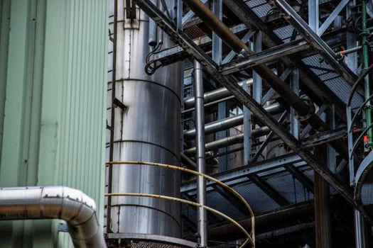
Process selection among dissolved air flotation (DAF), membrane bioreactor (MBR), and hybrid DAF-MBR tracks fab flow and solids load, not brand preference. DAF removes 92–97% TSS as pre-treatment (EPA 2024 performance range for well-run flotation), which cuts the solids shock on downstream biology. DAF alone does not meet GaN COD targets of 500–3,000 mg/L influent, so a biological polishing stage follows.
Standalone MBR units can reach over 95% COD removal in one compact footprint, yet CAPEX often sits at $2M–$20M and metal-rich TSS raises fouling risk without upstream solids cut. Hybrid DAF-MBR trains suit fabs over about 500 m³/h and can trim overall CAPEX by up to 20% versus oversized standalone MBR. With DAF cutting TSS first, MBR membrane life often extends past 5 years on the same chemistry. A typical train runs:
- Etching & Rinsing: Initial wastewater with high COD, TSS, and metals.
- Equalization Tank: Buffers flow and concentration swings.
- DAF System: Removes 92–97% of TSS and some colloids.
- MBR System: Achieves 95%+ COD removal and polishes effluent.
- Zero Liquid Discharge (ZLD): Evaporation or reuse when discharge permits require it.
For solids pre-treatment, DAF systems for GaN TSS pre-treatment pair with a packaged MBR Membrane Bioreactor Wastewater Treatment System when the fab wants one accountable process boundary.
What Are CAPEX and OPEX for GaN Semiconductor Wastewater Treatment?
GaN semiconductor wastewater treatment CAPEX scales mainly with flow, membrane material, and whether ZLD is mandatory; OPEX follows membrane replacement and chemicals. 2027 industry benchmarks place CAPEX near $2M for a 50 m³/h PVDF MBR and up to $40M–$50M for a 1,000 m³/h ZLD plant that still includes MBR/SiC stages. Hybrid DAF-MBR at flows over 500 m³/h can cut CAPEX by up to 20% versus a standalone MBR sized for raw TSS.
Annual OPEX is typically 60–70% membrane replacement plus chemicals for pH, coagulation, and nutrients. SiC modules cost about 2× more upfront than PVDF, yet deliver 30–40% lower OPEX and a 2–3 year payback on many 500+ m³/h fabs. Teams comparing full-fab water budgets should separate wastewater from UPW: typical UPW CAPEX for a semiconductor plant is a different cost center and must not be mixed into these wastewater figures when boards review the capex process for chip-fab wastewater scopes.
| System Size (m³/h) | Configuration | Estimated CAPEX | Estimated OPEX/Year | Typical Membrane Lifespan | Estimated Chemical Costs/Year |
|---|---|---|---|---|---|
| 50 | MBR (PVDF) | $2M | $250K–$400K | 2–3 years | $50K–$100K |
| 200 | MBR (SiC) | $8M–$12M | $400K–$600K | 5+ years | $75K–$150K |
| 500 | DAF-MBR (SiC) | $20M–$30M | $1M–$1.5M | 5+ years | $200K–$300K |
| 1,000 | ZLD (including MBR/SiC) | $40M–$50M | $3M–$5M | N/A (evaporation) | $500K–$800K |
Selection checklist before freezing the bid package:
- Peak and average flow (m³/h) with etch-dump coincidence factor.
- Influent COD, TSS, Ga, Al, As, pH band, and temperature (°C).
- Discharge permit vs on-site reuse/ZLD requirement.
- PVDF vs SiC membrane life and CIP chemical budget.
- Need for DAF pre-treatment when TSS exceeds about 200 mg/L sustained.
- Ion-exchange or adsorption polishing for Ga/As after biological treatment.
- Spare-module and media replacement lead times in the OPEX model.
Compliance Checklist: Meeting EPA, EU, and China GaN Discharge Limits
GaN fab effluent must clear metal limits that sit tighter than many generic industrial permits. EPA 40 CFR Part 469 lists Ga <1.0 mg/L, Al <0.2 mg/L, and As <0.1 mg/L for semiconductor manufacturing wastewater in the design packages most fabs circulate. EU and China programs often push Ga to 0.5 mg/L and As to 0.05 mg/L, which usually needs polishing beyond standard MBR.
The underlying US rule is older and narrower than those working numbers suggest. Part 469, titled the Electrical and Electronic Components Point Source Category, carries the Federal Register source citation 48 FR 15394 of April 8, 1983 and places its Semiconductor Subcategory in Subpart A (Cornell LII, 40 CFR Part 469). EPA’s official program page lists fluoride, arsenic, and organic compounds as the regulated pollutants, covering discharges from etching, cleaning, degreasing, cutting, and grinding (US EPA). EPA’s Effluent Guidelines Program Plan 15 (January 2023) completed a detailed study of the category, kept the rule unchanged, and continues monitoring PFAS discharges from the industry (US EPA). Treat the Ga/Al/As triplet as permit-specific numbers and verify them against the plant’s NPDES or local permit before fixing polishing scope.
Lime or caustic precipitation cuts bulk metals but may miss the lowest As/Ga targets. Ion exchange or advanced adsorption is then added for trace removal; ion exchange can reach about 99% removal of target metals, with higher OPEX from regenerant and media replacement. Pair precipitation, MBR, and selective polishing only after a metals mass balance at peak dump conditions—not average daily composite alone.
| Contaminant | EPA 40 CFR Part 469 | EU / China (typical) | Primary Treatment Path |
|---|---|---|---|
| Gallium (Ga) | <1.0 mg/L | 0.5 mg/L | Precipitation + ion exchange / adsorption |
| Aluminum (Al) | <0.2 mg/L | Often tighter locally | pH-controlled precipitation |
| Arsenic (As) | <0.1 mg/L | 0.05 mg/L | Ion exchange / advanced adsorption |
| COD | Permit-specific | Permit-specific | MBR (≥95% removal typical on designed loads) |
| TSS | Permit-specific | Permit-specific | DAF 92–97% then MBR polish |
Who This Is For / Who Should Look Elsewhere / Next Step
Process and utilities engineers sizing GaN or wide-bandgap fab wastewater at roughly 50–1,000 m³/h, who need membrane, DAF, and metal-polishing decisions tied to CAPEX bands, are the audience for this page. Look elsewhere if you only need municipal MBR primer material or UPW make-up design without a wastewater permit driver. For a duty-sized proposal on your dump schedule and metal limits, send the influent table through our GaN fab wastewater inquiry form.
Frequently Asked Questions
What is ZLD system capex for a semiconductor fab in 2027?
Budget $40M–$50M for a 1,000 m³/h ZLD train that still includes MBR or SiC stages, while a 50 m³/h PVDF MBR without evaporation runs about $2M, per 2027 benchmark ranges. Hybrid DAF-MBR at flows over 500 m³/h can cut CAPEX by up to 20% versus standalone MBR. Final price tracks peak dump coincidence, metal polishing depth, and membrane material more than nameplate average flow.
What CAPEX should a GaN fab budget for wastewater treatment?
Budget about $2M for a 50 m³/h PVDF MBR and $40M–$50M for a 1,000 m³/h ZLD train that still includes MBR or SiC stages, using 2027 benchmark ranges. Between those poles, a 200 m³/h SiC MBR sits near $8M–$12M and a 500 m³/h DAF-MBR near $20M–$30M. Final price tracks peak dump coincidence, metal polishing, and membrane material more than nameplate average flow.
When should a GaN plant choose SiC over PVDF membranes?
Choose SiC when pH routinely leaves the 3–11 PVDF window, temperature stays near 50–80°C, or CIP chemicals already dominate OPEX. SiC modules cost about 2× more upfront yet often cut annual OPEX 30–40% with 5+ year performance windows versus 6–12 month fouling on PVDF in hard GaN service. Payback commonly falls inside 2–3 years on 500+ m³/h plants.
Is DAF enough for GaN semiconductor wastewater?
No. DAF alone is a solids step: it can remove 92–97% TSS but does not meet high COD loads of 500–3,000 mg/L typical of GaN etch and rinse water. Use DAF as pre-treatment ahead of MBR or a hybrid DAF-MBR train, then add precipitation and ion exchange when Ga or As limits drive the permit.
Which discharge limits apply to gallium and arsenic?
Under EPA 40 CFR Part 469 framing used in this design basis, Ga is <1.0 mg/L and As is <0.1 mg/L, with Al at <0.2 mg/L, though EPA’s own program page names fluoride, arsenic, and organics as the Part 469 pollutants (US EPA). EU and China programs often require Ga at 0.5 mg/L and As at 0.05 mg/L. Confirm the governing permit early; polishing steps change when the tighter overseas numbers apply to an export-oriented fab.
How does GaN effluent compare with silicon fab wastewater?
GaN streams typically show COD 500–3,000 mg/L and TSS 200–1,500 mg/L, about 3–5× silicon ranges of COD 100–500 mg/L and TSS 50–200 mg/L, plus Ga/As that silicon lines usually lack. Temperature is also hotter (50–80°C vs 20–50°C), which shortens polymeric membrane life if equalization and material selection are weak.
How much equalization HRT does GaN wastewater need before DAF or MBR?
A 6–12 h equalization HRT at peak shift flow is the usual floor, because pH swings from 1 to 13 across etch and rinse dumps within one shift. Segregate dumps by tool family whenever daily mass loads differ by more than about 2×. Skip that split and PVDF modules fall into CIP every few months instead of holding the planned 6–12 month fouling window.