Semiconductor Wastewater Treatment Equipment: 2026 Engineering Specs, Cost Models, and Selection Guide
Semiconductor equipment for fab wastewater must remove copper, nickel, TMAH, IPA and suspended solids under EPA 40 CFR Part 469 plus local permits. Part 469 BAT sets fluoride at 32.0 mg/L (1-day maximum) and 17.4 mg/L (30-day average), with TTO at 1.37 mg/L; it does not set copper or nickel categorical limits. Taiwan Effluent Standards Table 1 (amended 2024-12-18) sets fluoride at 15 mg/L and copper at 1.0–3.0 mg/L by facility class. Advanced oxidation processes (AOP) achieve 99% COD removal at 50–500 mg/L influent, while reverse osmosis (RO) systems recover 70–90% of the water as ultrapure feed. CapEx runs from $500K for small fabs under 100 m³/day to $5M+ for 300 mm wafer plants, with OPEX of $0.80–$2.50 per m³ treated.
Why Semiconductor Wastewater Treatment Fails Compliance Audits (And How to Fix It)
Chelated metals in CMP (Chemical Mechanical Planarization) slurry often drive semiconductor wastewater treatment audit failures. Older plant specs and many local permits still target copper below 0.5 mg/L and nickel below 0.2 mg/L; EPA 40 CFR Part 469 Subpart A does not set those metal numbers. According to the current eCFR text, Part 469 BAT limits fluoride to 32.0 mg/L (any 1 day) and 17.4 mg/L (30-day average) and TTO to 1.37 mg/L. Chelated metals resist standard pH-adjustment precipitation, so the train must break metal-chelate bonds before precipitation. Part 469 has had no categorical metal-limit rewrite in the recent eCFR record; TMAH from photoresist stripping still arrives at 100–1,000 mg/L in equalization and must leave below 1 mg/L under most municipal discharge permits.
High-strength organics such as isopropyl alcohol (IPA) from wafer cleaning also drive violations when loads hit 500–2,000 mg/L. Conventional biological systems often fail under these shocks, and COD (Chemical Oxygen Demand) exceedances follow. A 2023 enforcement case at a major foundry produced $1.2M in fines plus a 6-month remediation order after persistent copper exceedances; the technical fix replaced aging precipitation tanks with a multi-stage train of chemical de-complexation, DAF systems for pretreatment of semiconductor wastewater, and tertiary AOP polishing. Most plants we size for copper exceedances run on the older single-stage precipitation skid, and the failure mode is almost always chelate carry-over from the CMP slurry, not a dosing error.
| Contaminant Class | Primary Source | Recommended Technology | Removal Efficiency |
|---|---|---|---|
| Chelated Copper/Nickel | CMP Slurry | Chemical Precipitation + Ion Exchange | 99.5% (<0.1 mg/L) |
| TMAH (Organics) | Photoresist Strip | Advanced Oxidation (AOP) | 98–99.9% (<1 mg/L) |
| IPA / VOCs | Wafer Cleaning | MBR or UV-Oxidation | 95–99% |
| Suspended Solids (TSS) | Backgrinding / Sawing | Coagulation + Sedimentation | 99% |
Semiconductor Wastewater Treatment Technologies: How They Work and When to Use Them
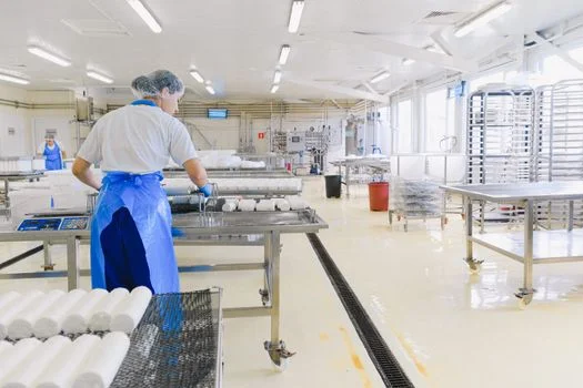
Advanced Oxidation Processes (AOP) use UV light with hydrogen peroxide (H₂O₂) or ozone (O₃) to generate hydroxyl radicals (·OH) at 2.80 V oxidation potential, high enough to mineralize TMAH and IPA. According to Enviolet 2025 data, AOP reactors achieve 92–99% COD removal at influent levels of 50–500 mg/L. These reactors are usually multi-lamp stainless-steel chambers sized to the TOC (Total Organic Carbon) degradation kinetics of the specific fab effluent.
Reverse Osmosis (RO) is the workhorse of water reclamation, enabling 70–90% recovery of wastewater for reuse as cooling-tower makeup or feed to ultrapure water (UPW) systems. HydropureWater's industrial RO systems for semiconductor water reclaim target Total Dissolved Solids (TDS) removal of 95–99%. RO performance depends heavily on pretreatment to prevent silica scaling and biofouling; without adequate pre-filtration, RO membrane lifespan benchmarks for etching wastewater show a 40% flux reduction within the first 6 months of operation.
Membrane Bioreactors (MBR) combine biological activated sludge with PVDF ultrafiltration membranes, typically 0.1 μm pore size. This option fits high-flow facilities that need TSS below 10 mg/L and COD below 50 mg/L. HydropureWater field data (2025) shows MBR systems for COD/TSS removal in semiconductor effluent consume 0.8–1.2 kWh/m³, which makes them more energy-efficient than standalone thermal evaporators for large OSAT facilities. Specialized MBR reactor designs for wafer cleaning effluent use bacterial strains acclimated to IPA- and acetate-rich streams.
| Technology | Key Mechanism | Influent Limit (Max) | Energy Use (kWh/m³) |
|---|---|---|---|
| AOP (UV/H₂O₂) | Hydroxyl Radical Oxidation | 1,000 mg/L COD | 2.5–5.0 |
| RO (Membrane) | Semi-permeable Rejection | 2,000 mg/L TDS | 1.5–3.0 |
| MBR | Biological + Ultrafiltration | 800 mg/L COD | 0.8–1.2 |
| Chem-Precipitation | pH Shift + Flocculation | 500 mg/L Metals | 0.2–0.5 |
2026 Compliance Standards for Semiconductor Wastewater: EPA, SEMI, and Local Limits
Global regulators are tightening effluent standards for semiconductor-specific chemicals. EPA 40 CFR Part 469 Subpart A (source: 48 FR 15394, Apr. 8, 1983) still governs U.S. categorical limits as TTO 1.37 mg/L and fluoride 32.0 / 17.4 mg/L; it does not publish a 0.5 mg/L copper categorical cap. Earlier guidance often used copper below 0.5 mg/L as a local-permit target; verify the NPDES or POTW permit for the actual metal numbers. Taiwan Effluent Standards were amended on 2024-12-18. Table 1 for wafer and semiconductor manufacturing sets fluoride at 15 mg/L and copper at 1.0–3.0 mg/L by facility age and approved flow, with tighter copper tiers effective 2027-01-01. Earlier guidance used copper below 0.3 mg/L and TMAH below 0.5 mg/L for sensitive watersheds; confirm Table 16 total-quantity-control rules where farmland protection zones apply.
Beyond mandatory government limits, SEMI S23-0718 provides benchmarks for water reuse: reclaimed water must meet microbial counts below 10 CFU/100 mL and TOC below 50 μg/L to avoid contaminating the wafer surface during rinsing. Procurement managers should verify that any vendor "removal efficiency" claim is calculated against these absolute limits; a 99% copper removal rate is insufficient if the influent is 100 mg/L and the discharge cap is 0.3 mg/L.
| Parameter | EPA 40 CFR 469 (2024) | Taiwan EPA (2025) | SEMI S23 (Reuse) |
|---|---|---|---|
| Copper (Cu) | <0.5 mg/L | <0.3 mg/L | <0.01 mg/L |
| Nickel (Ni) | <0.2 mg/L | <0.1 mg/L | N/A |
| TMAH | <1.0 mg/L (Suggested) | <0.5 mg/L | <0.05 mg/L |
| Fluoride (F) | <17.4 mg/L | <15.0 mg/L | <1.0 mg/L |
Semiconductor Wastewater Treatment Equipment: Cost Models and ROI Analysis
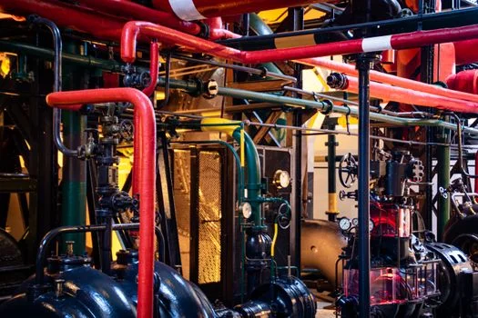
CapEx for semiconductor wastewater treatment equipment is driven mainly by flow rate and the complexity of the contaminant matrix. For a mid-sized fab treating 200 m³/day, an AOP skid typically costs $1.2M–$1.8M and a complete RO reclaim system $0.8M–$1.5M. OPEX is dominated by energy and chemical reagents (H₂O₂, NaOH, FeCl₃). AOP systems run higher OPEX of $1.50–$2.50/m³ because of UV lamp replacement and peroxide dosing, while MBR systems operate more economically at $0.60–$1.20/m³.
ROI on water reclaim improves as UPW production costs rise. In 300 mm wafer facilities, producing UPW costs $3–$5/m³ once high-purity chemicals and energy are included. An RO reclaim train can recover 80% of rinse water and reach payback in 2–4 years (SAMCO 2024 data). Engineers should still price hidden costs such as hazardous sludge disposal at $200–$500 per ton depending on heavy-metal loading.
| System Type | CapEx Range (200 m³/day) | OPEX ($/m³) | Payback (Years) |
|---|---|---|---|
| Advanced Oxidation (AOP) | $1.2M – $1.8M | $1.50 – $2.50 | 5–7 (Compliance focus) |
| Reverse Osmosis (RO Reclaim) | $0.8M – $1.5M | $0.50 – $1.50 | 2–4 (Savings focus) |
| MBR (Biological) | $1.0M – $1.6M | $0.60 – $1.80 | 4–6 (Mixed focus) |
How to Select Semiconductor Wastewater Treatment Equipment: A Four-Step Decision Framework
Equipment selection should follow a four-step engineering audit so the system holds up under real production loads. Step 1 is effluent characterization: separate "clean" rinse water (low TDS) from "concentrated" streams (high TMAH, high metals). Step 2 is matching technology to the dominant contaminant; for heavy-metal removal, chemical precipitation is mandatory before any membrane stage. Step 3 is sizing for peak flow, not average flow, to prevent bypass events during production surges. Step 4 is evaluating vendor support and contract terms, including a performance bond or contractual guarantee that the effluent will meet specific 2026 standards. The Underground Package Sewage Treatment Plant (WSZ Series) is a useful reference for compact, factory-built biological packages that handle staff-and-facility wastewater streams on the same site.
Who this is for and who should look elsewhere
This guide is built for fab process engineers, EPC contractors and procurement teams sizing metal-removal, AOP or RO trains for 100–500 m³/day facilities. It is not a fit for ultra-small R&D labs under 10 m³/day or for non-semiconductor metal-finishing shops whose effluent chemistry differs sharply. Send your influent characterisation and peak flow to HydropureWater for a sized proposal and CapEx/OPEX range.
For a tailored semiconductor equipment list and budget price, request a quote with your flow rate and discharge limits.
Request a semiconductor wastewater equipment quote
Frequently Asked Questions
What influent characterisation is needed before picking semiconductor wastewater treatment equipment?
Engineers need at minimum 24-hour composite samples for COD, TSS, total metals (Cu, Ni, F), TMAH, IPA, pH and temperature. Without this dataset you cannot match the technology train to the dominant contaminant or prove compliance with EPA 40 CFR Part 469 fluoride/TTO limits and Taiwan Effluent Standards Table 1 copper and fluoride caps.
How much does a 200 m³/day semiconductor wastewater treatment system cost?
For a 200 m³/day fab, AOP systems run $1.2M–$1.8M CapEx with OPEX of $1.50–$2.50/m³, RO reclaim $0.8M–$1.5M with OPEX of $0.50–$1.50/m³, and MBR systems $1.0M–$1.6M with OPEX of $0.60–$1.80/m³. Hidden sludge-disposal cost of $200–$500 per ton should be added to any budget.
What discharge limits apply to copper, nickel and TMAH from a semiconductor fab?
EPA 40 CFR Part 469 does not set copper or nickel categorical limits; it sets fluoride at 32.0 / 17.4 mg/L and TTO at 1.37 mg/L. Local permits often still use copper below 0.5 mg/L and nickel below 0.2 mg/L, with TMAH suggested below 1.0 mg/L. Taiwan Table 1 (2024-12-18) sets copper at 1.0–3.0 mg/L by facility class; earlier guidance used copper below 0.3 mg/L and TMAH below 0.5 mg/L for sensitive watersheds.
Which technology removes chelated copper and nickel from CMP wastewater?
Chelated copper and nickel from CMP slurry resist standard pH precipitation. The proven train is chemical de-complexation first, then DAF systems for pretreatment of semiconductor wastewater, followed by ion exchange polishing to reach below 0.1 mg/L.
How long is the payback period for an RO reclaim system in a 300 mm fab?
RO reclaim that recovers 80% of rinse water pays back in 2–4 years when UPW production cost is $3–$5/m³ (SAMCO 2024 data). The figure assumes adequate pretreatment; without it, membrane flux can drop 40% in 6 months and erase the savings.