Third-generation semiconductor fabs (GaN/SiC) generate wastewater with unique contaminants like TMAH, urea, and heavy metals (arsenic, chromium), requiring hybrid treatment systems to achieve zero liquid discharge (ZLD). A 2026 engineering blueprint combines membrane bioreactors (MBR) with advanced oxidation processes (AOP) and reverse osmosis (RO) to remove 99.9% of contaminants, reducing water consumption by 95% and cutting operational costs by 30% compared to conventional systems. CAPEX ranges from $5M–$20M depending on fab size and recovery targets.
Why Third-Generation Semiconductor Wastewater Is Harder to Treat Than Silicon
Gallium Nitride (GaN) and Silicon Carbide (SiC) fabrication processes utilize high concentrations of tetramethylammonium hydroxide (TMAH) and urea, creating a chemical oxygen demand (COD) profile that is significantly more resistant to standard aerobic treatment than traditional silicon-based effluents. While silicon fabs primarily deal with hydrofluoric acid and standard photoresist strippers, 3rd-generation fabs introduce low molecular weight organics (LWOs) that bypass conventional ultrapure water (UPW) reclamation loops (per Dr. Westerhoff’s research). These LWOs, specifically TMAH and acetone, require targeted mineralization to prevent build-up in recycled water streams.
Heavy metal concentrations in GaN/SiC production—including arsenic, chromium, and nickel—often exceed silicon fab limits by 5–10 times. For instance, the etching of GaN layers releases gallium and arsenic complexes that are difficult to precipitate using standard alum or ferric coagulants. water consumption in these facilities is notably higher; DuPont 2025 data indicates that a 12-inch GaN wafer requires 10–15 m³ of water, compared to 8–10 m³ for traditional silicon wafers. This increased demand, coupled with stricter discharge standards like China’s GB8978-2025, necessitates a shift from "treat-and-discharge" to "treat-and-reuse" models.
The physical nature of the waste also poses engineering challenges. GaN/SiC grinding and polishing (CMP) processes generate finer, more abrasive particulates than silicon. These sub-micron particles can clog standard filtration membranes 40% faster, leading to frequent backwashing and reduced flux. Without specialized pretreatment, such as DAF systems for semiconductor pretreatment, downstream reverse osmosis units face terminal fouling within weeks of commissioning.
| Parameter | Traditional Silicon Fab | 3rd-Gen (GaN/SiC) Fab | Treatment Challenge |
|---|---|---|---|
| Primary Organics | IPA, Photoresist | TMAH, Urea, Acetone | LWOs resist biological decay |
| Heavy Metals | Copper, Tin | Arsenic, Chromium, Nickel | 5-10x higher toxicity levels |
| Water Usage | 8–10 m³/wafer | 10–15 m³/wafer | Higher hydraulic loading |
| Particulate Size | 1.0–5.0 μm | 0.1–0.8 μm | Rapid membrane pore clogging |
| TMAH Concentration | <50 mg/L | 100–500 mg/L | Requires AOP for mineralization |
Hybrid Process Design: MBR + AOP + ZLD for 99.9% Contaminant Removal
A 2026 engineering blueprint for a third-generation semiconductor wastewater treatment project utilizes a multi-stage hybrid approach where advanced oxidation serves as the critical bridge between biological treatment and high-pressure membrane separation. This design is engineered to handle the fluctuating loads typical of batch-processing GaN lines while maintaining a 99.9% removal efficiency for regulated toxins.
Stage 1: Pretreatment and Solid Separation
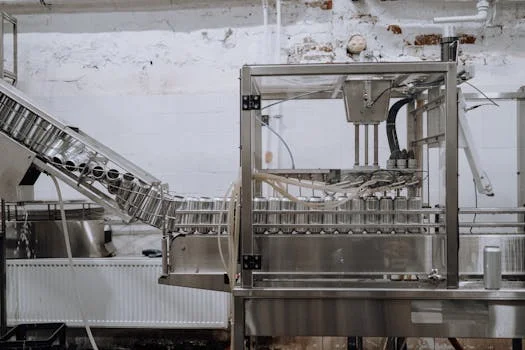
The process begins with rotary mechanical bar screens (GX Series) to remove over 95% of total suspended solids (TSS). These screens feature a 0.5–2 mm gap and capacities ranging from 10–500 m³/h, protecting downstream pumps from the abrasive SiC slurry. In cases of high surfactant loads, a DAF system is integrated to lift emulsified oils and fine particulates before they reach the biological stage.
Stage 2: Biological Mineralization (MBR)
The core of the organic removal process is an MBR system for semiconductor wastewater utilizing PVDF flat-sheet membranes (DF Series). These membranes operate at a pore size of 0.1 μm with a flux of 15–25 LMH. The MBR combines activated sludge treatment with ultrafiltration, maintaining a high Mixed Liquor Suspended Solids (MLSS) concentration of 8,000–12,000 mg/L. This allows for the degradation of urea and complex nitrogen compounds that would otherwise pass through standard clarifiers.
Stage 3: Advanced Oxidation Process (AOP)
To address TMAH and other LWOs, the system employs UV/H₂O₂ or ozone-based AOP. This stage generates hydroxyl radicals (.OH) that break the stable C-N bonds in TMAH, achieving 98–99.5% removal at influent concentrations of 5–10 mg/L. This is essential for protecting the RO membranes in Stage 4 from organic biofouling and ensuring the final effluent meets reuse standards for cooling towers.
Stage 4 & 5: RO and ZLD Evaporation
High-rejection reverse osmosis (RO) membranes target heavy metals, achieving 99.9% removal for arsenic and 99.8% for chromium. The RO permeate is typically diverted for facility reuse, while the concentrate is sent to a Mechanical Vapor Recompression (MVR) evaporator. This final ZLD stage achieves 95–98% total water recovery, leaving only a dry salt cake for hazardous waste disposal.
| Process Stage | Equipment/Technology | Key Performance Metric | Target Contaminant |
|---|---|---|---|
| Pretreatment | Rotary Screens / DAF | 95% TSS Removal | SiC Slurry, Particulates |
| Biological | MBR (PVDF 0.1 μm) | HRT: 12-18 Hours | Urea, Ammonia, COD |
| Oxidation | UV/H₂O₂ AOP | 99% TMAH Removal | LWOs, Resistant Organics |
| Desalination | High-Pressure RO | 99.9% As Removal | Arsenic, Chromium, TDS |
| ZLD | MVR Evaporator | 98% Water Recovery | Concentrated Brine |
Cost Breakdown: CAPEX, OPEX, and ROI for Semiconductor ZLD Systems
Capital expenditure (CAPEX) for a 3rd-generation semiconductor ZLD system typically ranges from $5 million to $20 million for facilities processing 50–500 m³/h. The cost structure is heavily influenced by the required recovery rate; moving from 70% reuse to 95% ZLD increases CAPEX by approximately 40% due to the inclusion of thermal evaporation units. According to Zhongsheng field data (2025), the CAPEX breakdown generally follows a 40/30/20/10 ratio: 40% for core equipment (MBR, AOP, RO), 30% for mechanical and electrical installation, 20% for process engineering and automation, and 10% for environmental permitting and commissioning.
Operational expenditure (OPEX) fluctuates between $0.50 and $1.20 per cubic meter of treated water. Energy consumption is the primary driver, accounting for 40% of the OPEX, particularly in the MVR and high-pressure RO stages. Chemicals, including precise chemical dosing for semiconductor wastewater (antiscalants, pH adjusters, and hydrogen peroxide), account for 30%. Labor and maintenance, including membrane replacement every 3–5 years, make up the remaining 30%.
The return on investment (ROI) is realized through three primary channels: reduced potable water procurement costs, eliminated discharge fees, and risk mitigation against regulatory fines. In water-stressed regions like Arizona or Northern China, potable water costs can exceed $2.50/m³. A case study of a $417M MWH plant demonstrated that achieving 30% water reuse alone reduced potable water purchases by $12 million annually, leading to a system payback period of 3–5 years. For smaller GaN fabs, the ROI is often driven by compliance; avoiding a single $100,000 regulatory fine for arsenic non-compliance significantly alters the TCO (Total Cost of Ownership) model.
| System Type | CAPEX (500 m³/h) | OPEX ($/m³) | Water Recovery % | Estimated ROI |
|---|---|---|---|---|
| MBR Only | $3M – $6M | $0.25 – $0.45 | 0% (Discharge only) | N/A (Compliance) |
| MBR + RO (Reuse) | $7M – $12M | $0.45 – $0.75 | 60% – 75% | 4 – 6 Years |
| Hybrid ZLD (MBR+AOP+RO+MVR) | $15M – $25M | $0.90 – $1.50 | 95% – 99% | 3 – 5 Years* |
*ROI for ZLD includes savings from zero discharge fees and high-cost water procurement.
Compliance and Discharge Standards: China GB8978 vs. Global Limits
The China GB8978-2025 standards for semiconductor manufacturing impose an arsenic limit of ≤ 0.1 mg/L, which is five times more stringent than the general industrial discharge limits often applied to silicon fabs in other jurisdictions. This standard specifically targets the high-toxicity waste streams of GaN production. COD limits are capped at 50 mg/L, a threshold that is nearly impossible to reach with biological treatment alone when TMAH is present, necessitating the use of CMP wastewater treatment solutions that incorporate oxidation.
In the United States, the EPA 40 CFR Part 469 sets the federal floor for semiconductor discharge, focusing heavily on TMAH (≤ 1 mg/L) and fluoride (≤ 4 mg/L). However, local municipal limits in chip-making hubs like Austin or Portland often impose stricter "local limits" on total toxic organics (TTO). In the European Union, the Industrial Emissions Directive (IED) is increasingly mandating ZLD for new fabs located in water-stressed basins, moving beyond simple concentration limits to mass-balance-based permits that limit the total kilograms of pollutants discharged per year.
Hybrid systems (MBR + AOP) are designed to provide a 20% safety margin against these standards. By mineralizing organics and utilizing dual-barrier membrane separation, these systems ensure that even during process upsets in the fab, the final effluent remains well below the regulatory "red line." For more on high-recovery systems, see our ZLD engineering blueprints for IC fabs.
| Pollutant | China GB8978-2025 | US EPA (40 CFR 469) | EU IED (Baseline) |
|---|---|---|---|
| Arsenic (As) | ≤ 0.1 mg/L | ≤ 2.09 mg/L (TTO) | ≤ 0.15 mg/L |
| Chromium (Cr) | ≤ 0.5 mg/L | Local Limits Apply | ≤ 0.5 mg/L |
| TMAH | Included in COD | ≤ 1.0 mg/L | Site-Specific |
| Fluoride (F) | ≤ 10 mg/L | ≤ 4.0 mg/L | ≤ 15 mg/L |
| Ammonia (NH3-N) | ≤ 10 mg/L | N/A | ≤ 15 mg/L |
Decision Framework: How to Select the Right Wastewater Treatment System for Your Fab

Selecting a wastewater treatment system for GaN/SiC lines requires a five-step evaluation framework that prioritizes wastewater characterization via bench-testing to prevent irreversible membrane fouling from sub-micron particulates. Engineers must move away from generic "packaged" plants and toward modular, site-specific designs that account for the unique chemical footprint of 3rd-generation semiconductors.
- Step 1: Define Water Reuse Goals: Determine if the facility requires 30% recovery (for scrubbers/cooling) or 95%+ ZLD. This decision dictates the inclusion of MVR evaporation.
- Step 2: Wastewater Characterization: Conduct comprehensive sampling for TMAH, urea, and sub-micron TSS. Pilot projects (typically costing $50K–$200K) are mandatory to determine the specific flux rates for MBR membranes.
- Step 3: Decision Matrix Evaluation: Compare MBR-only vs. Hybrid (MBR+AOP+RO) designs. If TMAH is >50 mg/L, AOP is non-negotiable.
- Step 4: Vendor Experience: Evaluate vendors based on semiconductor-specific references. A vendor experienced in municipal sewage will likely fail to address the abrasive nature of SiC particulates.
- Step 5: TCO Calculation: Use a 5-year Total Cost of Ownership model that includes membrane replacement, chemical consumption, and sludge disposal costs.
Common mistakes in system selection include underestimating the impact of GaN etching byproducts on membrane longevity. Without a robust precise chemical dosing system to manage pH and coagulant addition, the fine particulates will bypass primary clarifiers and cause irreversible "internal" fouling of the MBR fibers. Engineers should also verify that the MBR system can handle high nitrogen loads from urea without requiring massive external carbon sources.
| Selection Factor | MBR-Only System | Hybrid AOP + RO System | Full ZLD System |
|---|---|---|---|
| Target Fab Size | Small R&D Lines | Mid-Scale Production | Large-Scale Giga-Fabs |
| TMAH Removal | Low (20-40%) | High (99%+) | Complete Mineralization |
| Heavy Metal Risk | Moderate | Low (Membrane Barrier) | Zero Discharge |
| Space Requirement | Compact | Moderate | High (requires evaporator) |
| Regulatory Safety | Low Margin | High Margin | Absolute Compliance |
Frequently Asked Questions
What is the biggest challenge in treating GaN/SiC wastewater?
The primary challenge is the presence of low molecular weight organics (LWOs) like TMAH and urea. These compounds are resistant to conventional treatment and require advanced oxidation (AOP) to achieve 99%+ removal, as standard biological systems often struggle with the high nitrogen and COD stability of these chemicals.
How much does a semiconductor ZLD system cost?
For a third-generation semiconductor wastewater treatment project, CAPEX ranges from $5M–$20M for 50–500 m³/h systems. OPEX typically falls between $0.50 and $1.20 per cubic meter, depending on energy costs and the volume of chemicals required for neutralization and oxidation.
Can MBR systems handle GaN/SiC wastewater without pretreatment?
No. Fine particulates from the etching and CMP processes in GaN/SiC production are highly abrasive and small enough to clog membrane pores within weeks. Pretreatment using rotary screens or DAF systems is mandatory to protect the MBR and RO membranes.
What are the water reuse targets for leading semiconductor fabs?
Leading global fabs aim for 95%+ recovery. While 30–50% of water is typically reused in low-grade applications like cooling towers and scrubbers (as seen in the MWH case study), advanced hybrid systems allow for high-purity water to be cycled back into the UPW makeup stream.
How do I ensure compliance with China GB8978-2025?
Compliance requires a multi-barrier approach. Hybrid systems combining MBR (for organics), AOP (for TMAH), and RO (for heavy metals like arsenic and chromium) provide a 20% safety margin, ensuring all parameters stay below the strict 2025 limits.